
Search results for Hybrid Bonding
Industry
Applied Materials, BE Semiconductor Industries expand EPIC Center cooperation for AI packaging
Applied Materials said on Thursday it will expand its strategic partnership with BE Semiconductor Industries, with BESI joining Applied\'s EPIC Center as an innovation partner. The companies plan to widen cooperation beyond their joint development program launched in 2020 to cover new interconnect structures and applications. They will jointly optimise process and assembly solutions across advanced packaging, from wafer-level hybrid bonding to panel-scale integration, aiming to deliver jointly optimised results to customers earlier.

Industry
Samsung Electronics bets on zHBM by stacking memory on accelerators
Samsung Electronics is preparing a two-track strategy of conventional HBM5 and its zHBM concept as it seeks to regain leadership in high-bandwidth memory. The company is shifting to a design that stacks HBM directly on top of AI accelerators, removing the interposer that links logic and memory side-by-side. Samsung targets 230 percent higher bandwidth and 70 percent lower power than HBM4E. Commercialisation will hinge on heat management and wafer hybrid-bonding yields.
AI & Enterprise
LG to hold \'LG Spark 2026\' in Magok, unveil new Physical AI and AIDC technologies
LG will hold \'LG Spark 2026\' at LG Sciencepark in Magok, Seoul, from Sept. 7 to 17, it said on Thursday. The event will run five programs focused on spreading AI innovation and transformation cases. LG will showcase 41 new R&D technologies, including Physical AI, AIDC and mobility. It will also present 68 AX cases, share Exaone applications and plans, hold a developer conference with global firms, and run mentoring and experience programs for students.
-

Industry
AMAT says AI chip performance hinges on data movement, solution is 3D scaling
-
Industry
SK Hynix wraps up LTA talks with about 10 customers including core clients, negotiating 2027 volumes and prices
-

Industry
HBM4 thickness rule eased, MR-MUF and TC-NCF upgrade race enters new phase
-

Industry
Semiconductor boom, but South Korea\'s chip equipment exports to China fall
-
Industry
Applied Materials expands packaging equipment lineup to boost HBM, chiplet yields
-
Industry
HBM beyond 16 layers brings memory makers\' hybrid bonding shift into view
-

Industry
Justem secures 30 billion won semiconductor policy funding from KDB
-
Industry
Dutch chip equipment maker Besi sees surge in hybrid bonding orders on AI infrastructure investment
-
Industry
Lam Research, Applied Materials consider acquiring Dutch chip equipment maker BESI
-
Industry
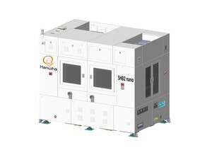
Hanwha Semitec completes development of second-generation hybrid bonder
-

Industry
European semiconductor technology firms turn to South Korea
-

Industry
Korean HBM equipment makers target Japan\'s semiconductor market