
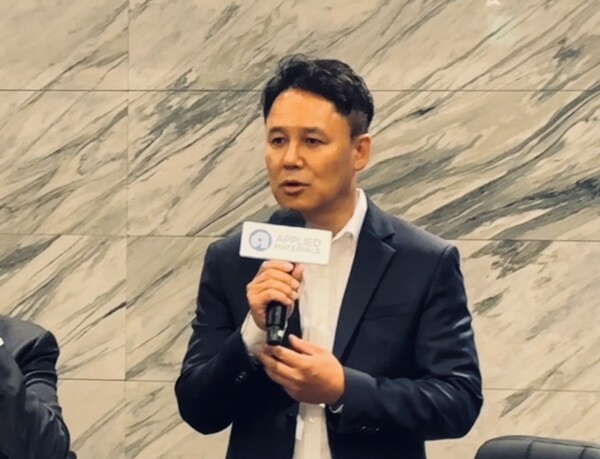
Applied Materials (AMAT) pointed to data movement efficiency, not computing speed, as the key bottleneck in artificial intelligence (AI) semiconductor performance. It is responding with 3D scaling (miniaturisation) technology across areas ranging from DRAM to high bandwidth memory (HBM) and system integration. Mukund Srinivasan, group vice president at Applied Materials, said at a media briefing in Seoul on Aug. 31 that as AI models evolve to be more compute-intensive, power consumption is rising sharply. He said the industry solution is 3D scaling.
He said the so-called "memory wall", in which processor performance improves rapidly while memory fails to keep pace and constrains overall system performance, has emerged as a new challenge as AI spreads. Srinivasan split the elements of AI semiconductors into three: logic chips that handle computation, memory that stores and supplies data, and packaging that places the two close together. He said 3D scaling is under way in logic through gate-all-around (GAA) and FinFET structures, in memory through HBM made by vertically stacking DRAM, and in packaging through 2.5D and 3D structures.
He added that capacity expansion across the ecosystem also needs to proceed in parallel because semiconductor demand far exceeds supply. Applied Materials' fiscal 2026 third-quarter revenue rose 25 percent from a year earlier to $9.12 billion. The company said demand for materials engineering solutions driven by the spread of AI was behind the revenue growth.
Applied Materials is pursuing a strategy of applying transistor and wiring technologies proven in leading-edge logic processes to DRAM to raise speed and energy efficiency. A representative example is an epitaxy process that selectively grows boron-doped silicon germanium (SiGe) in the source and drain regions of DRAM peripheral-circuit transistors.
Channel strain created in the process improves DRAM performance and power consumption. As use of extreme ultraviolet (EUV) lithography expands, the number of cells and peripheral-circuit transistors integrated on a chip is increasing, along with the number of copper wiring layers. Peripheral-circuit transistors are trending toward a shift from high-k metal gate (HKMG) to FinFET. Srinivasan stressed that improvements in DRAM performance depend on how quickly materials engineering technologies first implemented in leading-edge foundry and logic are adopted.
◆ HBM process shifts from micro-bumps to hybrid bonding
HBM is made by vertically stacking DRAM using through-silicon vias (TSV) to increase bandwidth. As a result, HBM DRAM die sizes can be up to 2 times those of standard DRAM because of TSV channel area, requiring 3 to 4 times more wafers to achieve the same capacity. Srinivasan said that for HBM to scale while maintaining energy efficiency, stacking based on micro-bumps must shift to hybrid bonding.
Hybrid bonding can effectively eliminate the gap between dies, improving thermal performance and boosting input-output (I/O) density to about 1,000,000 per square millimetre. For this, Applied Materials last year introduced with partners a die-to-wafer hybrid bonding system called Kinex. The company said the equipment cuts waiting time between processes to 1 hour from 13 hours. Applied projected advanced packaging revenue would grow more than 70 percent in 2026 and is pushing to acquire NEXX to strengthen panel-level technology.
Work is also under way to bundle memory, computation and connectivity into a single system. Co-packaged optics (CPO) integrates electronic and optical chips at the package level and transmits data using optical signals. Applied Materials is aiming to develop panel interposers up to a 600x600mm standard after 310x310mm and 510x515mm. It added that existing 300mm round wafers suffer edge losses when producing square interposers, limiting output to 4 to 5 per wafer.
The company said larger panel sizes instead increase the number of interposers that can be produced, improving productivity and cutting costs. Srinivasan said logic devices have more than 2,000 process steps and memory devices have more than 1,200, and that the steps interact with one another. He said the innovation challenge is to optimise them together by connecting the whole, rather than optimising each process individually.
It also plans to actively join cooperation with South Korean companies to reduce gaps in semiconductor equipment. The company said Samsung Electronics and SK Hynix are founding partners of Applied's EPIC (Equipment and Process Innovation and Commercialisation Center), and that through Applied Collaboration Center Korea (ACC Korea) in Osan, Gyeonggi Province, it is conducting joint technology development and mass-production verification with local customers. Park Kwang-sun (박광선), head of Applied Materials Korea, said it is working to ensure there are no gaps in personnel and technology support as Samsung Electronics and SK Hynix expand fabs to places such as Taylor, Texas.
 Seok Dae-geon
d2dg@d-today.co.kr
Seok Dae-geon
d2dg@d-today.co.kr