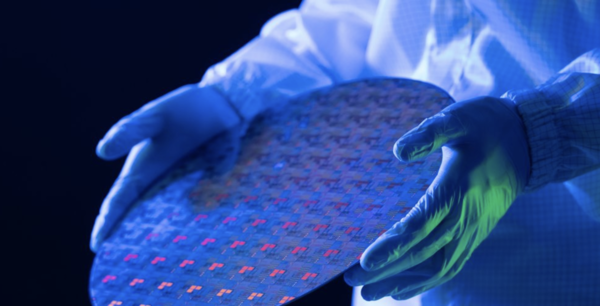
European semiconductor technology firms are choosing to head to South Korea. With an insufficient base at home to validate mass production, Samsung Electronics and SK Hynix’s most advanced lines have emerged as an alternative. South Korea is changing status from an equipment-importing country to a partner for joint technology development.
In the past, South Korea was a market that imported and used completed equipment from the United States, Japan and the Netherlands. But the recent trend is changing. The structure is shifting to one in which European firms with foundational technologies come directly to collaborate with South Korean companies from the development stage. Analysis is emerging that South Korea is rising beyond a simple manufacturing hub to become a central site for validating next-generation semiconductor technology.
There are structural factors behind European firms’ move to South Korea. Europe has world-class research institutes such as Belgium’s IMEC and Germany’s Fraunhofer, giving it foundational technology strength, but it lacks an integrated device manufacturer (IDM) to validate these technologies on a mass-production line. According to the Korea-EU semiconductor R&D cooperation center, a reference that a technology is "being tested on Samsung or SK lines" acts for European startups as a guarantee that helps attract investment.
Developments within Europe are also spurring their move to South Korea. Last year, Broadcom withdrew a planned $1 billion investment in a semiconductor assembly and test plant (ATP) in Spain. Spain ran a 12.25 billion euro semiconductor promotion programme, but failed to attract large manufacturing facilities. As EU Chips Act funds concentrate on existing strongholds such as Dresden in Germany, European technology firms are seeking alternative markets for mass-production validation.
Entry into the U.S. and Chinese markets is also difficult. Exports to China are limited due to U.S.-China tensions, and the United States has a strong domestic ecosystem centred on Intel and Micron. By contrast, South Korea is the only country that holds the most advanced processes in both memory and foundry at the same time. Industry assessments say South Korea, not Taiwan, is the only market where DRAM and NAND memory and logic foundry can be validated in one place.
◆"Tackling hard problems existing equipment cannot solve with niche technologies"
European firms coming to South Korea have niche technologies to solve technical challenges facing Samsung Electronics and SK Hynix. They broadly fall into next-generation packaging and new materials, metrology for ultra-fine processes, and design simulation.
In next-generation packaging, glass substrate technology is drawing attention. With existing plastic substrates, it is difficult to overcome limits in thermal management and signal transmission for high-performance computing (HPC) chips. European firms with materials technology needed to commercialise glass-core substrates being pursued by Samsung Electro-Mechanics and SKC Absolics are set to visit South Korea to coincide with Semicon Korea, which will be held next month.
Demand is also strong in ultra-fine process metrology. As 3D NAND stacks exceed 300 layers, technology to inspect whether the inside of deep, narrow holes is coated uniformly has become essential. Finnish and Spanish firms that have technology to measure thin films in high aspect ratio (HAR) structures in a non-destructive manner, and wavefront phase imaging technology that measures nanoscale unevenness on wafer surfaces at ultra-high speed, are knocking on the South Korean market.
Demand for design verification is also rising. In processes of 2 nanometres and below, mask production costs reach tens of billions of won, making it key to reduce trial and error. An Austrian firm with 3D TCAD simulation technology that predicts physical operation on computers before making an actual chip is also reported to be sounding out cooperation with Samsung Foundry and domestic fabless companies.
HBM, or high-bandwidth memory process advancement, has also become an opportunity for European firms. As processes such as TSV, or through-silicon via, and hybrid bonding become more complex, challenges that are difficult to solve with existing equipment are increasing. Moves by South Korean companies to diversify their materials, parts and equipment supply chains after Japan’s export curbs in 2019 are also opening doors for European small and medium-sized firms.
The EU Business Hub, which links these parties, plans to provide an opportunity for both European and South Korean companies to expand their global networks through events such as "Semiconductor Korea 2026". An industry official said, "How much European firms’ technology will translate into actual results is the key," and added, "For domestic semiconductor materials, parts and equipment firms, they are potential competitors but could also become partners for entering Europe through technology alliances."