As demand grows for 3D stacking technology in the AI chip equipment market, Applied Materials unveiled six new tools at once spanning advanced packaging and DRAM processes. Applied Materials said on Sunday it announced a lineup of semiconductor manufacturing systems needed to implement HBM and chiplet architectures.
According to the company, AI computing is facing a “memory wall” in which bandwidth and memory capacity fail to keep pace as model sizes grow and data throughput increases. It said key ways to break through include high-bandwidth memory, or HBM, which stacks DRAM chips vertically and connects them with through-silicon vias (TSV), and 3D stacking technology. These structures boost performance but also increase process complexity.
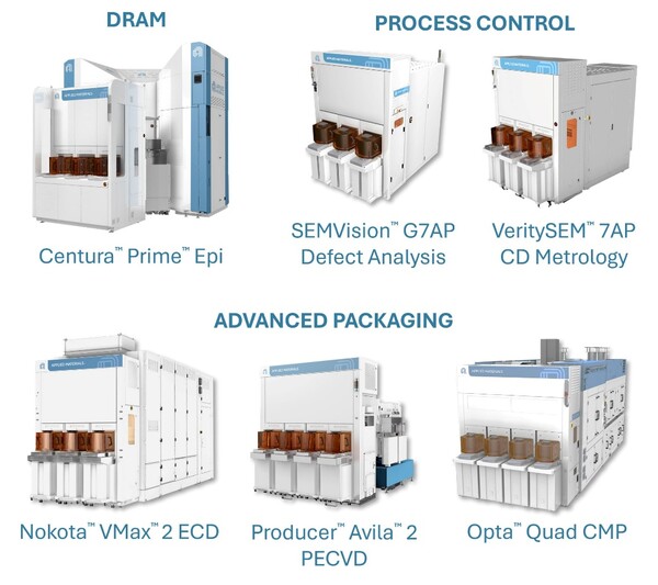
The first of the new tools is Opta Quad, a chemical mechanical planarization (CMP) system dedicated to advanced packaging. The system controls thickness in real time during wafer polishing to improve uniformity. Surface flatness is essential to secure yield in hybrid bonding that joins copper wiring and dielectric films from two chips at once. The Nokota Vmax 2 electrochemical deposition (ECD) system delivers high-precision copper plating from TSV fill through micro-bump formation, and corrects variation tied to circuit layouts using adaptive pattern tuning (APT) technology.
The Producer Avila 2 plasma-enhanced chemical vapor deposition (PECVD) system suppresses deformation in HBM dies thinned to about one twenty-fifth of a standard wafer thickness. It deposits dielectric films with balanced internal stress around TSVs, enabling stable bonding for highly stacked HBM with 12 layers, 16 layers or more.
Prabu Raja said Applied’s leadership in dielectric CVD, ECD and CMP and its process integration expertise would provide a key foundation for customers to scale 3D stacked structures with stability and high yields.
In the e-beam metrology segment, it introduced two tools, VeritySEM 7AP and SEMVision G7AP. In advanced packaging, a single defect can lead to scrapping an entire HBM stack, making precision inspection a strategic task. VeritySEM 7AP provides measurement sensitivity below 10 nanometers even on severely warped substrates, and SEMVision G7AP automatically classifies defects across silicon, organic and glass substrates. The company said leading memory and logic manufacturers have already adopted SEMVision G7AP.
For DRAM processes, it unveiled an upgraded Centura Prime epi system. The company introduced epitaxy technology previously used in logic semiconductors into DRAM peripheral transistors, selectively growing silicon germanium (SiGe) and silicon phosphorus (SiP) in source and drain regions to raise drive current and power efficiency. It also said the tool cuts installation footprint by 20 percent from existing systems, accelerating capacity expansion in fabs with limited space.
Keith Wells (키스 웰스), vice president of Applied Materials’ Imaging and Process Control Group, said VeritySEM 7AP and SEMVision G7AP extend Applied’s proven wafer fab expertise into packaging. He said they were purpose-designed from the start to address substrate characteristics and defect challenges unique to 3D architectures.