Search results for 2.5D packaging
Industry
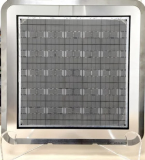
As AI chips grow, packaging substrates shift from round wafers to square panels
As AI chips grow in area, investment is starting at home and abroad to switch packaging bases from round wafers to large square substrates. Using square panels can process 5 to 6 times more chips at once than wafers, raising area utilisation to 87 percent from 57 percent. Competition is also intensifying between Taiwan and South Korean companies over panel-level packaging, a process that reassembles cut chips on a panel and builds moulding and redistribution layers.

Industry
ADTechnology wins chiplet design order for U.S. AI datacenter chips
ADTechnology said on Monday it signed a 40 billion won turnkey contract with a U.S. AI fabless company to develop and supply chiplets for a datacenter high-performance computing system-on-chip. The company will handle the full process from design to tape-out and mass production based on Samsung Foundry\'s 4-nanometre process. The project targets an integrated SoC chiplet combining HBM and AI accelerator logic, with tape-out aimed for the fourth quarter of 2026.
Industry
Nvidia seen reverting Rubin CPX memory to HBM from GDDR7
Market expectations are growing that Nvidia could switch the memory in its next-generation AI inference accelerator, Rubin CPX, from GDDR7 back to high-bandwidth memory. The view is driven by assessments that large-scale production inference workloads require more bandwidth and capacity than GDDR7 can efficiently provide. Rising inference demand cited by CEO Jensen Huang and comments on supply constraints have added momentum. A switch would require redesign and could affect HBM supply-demand outlooks.