Search results for IEDM
Industry
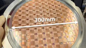
Foundry chip market shifts from shrinking nodes to packaging as stacking and chiplets become battleground
The semiconductor industry is shifting its technology race from shrinking process nodes to packaging as scaling approaches physical limits. Companies are increasingly relying on 2.5D and 3D stacking and chiplets to meet performance, power and bandwidth demands, driving changes across the value chain that includes IP, libraries and EDA tools. Memory makers SK hynix and Samsung Electronics are advancing their packaging technologies. Intel has also demonstrated GaN-on-silicon chiplet technology and integration with silicon digital control circuits.
Industry
KAIST develops \'smart door\' semiconductor structure to sharply expand storage capacity
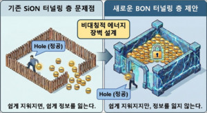
KAIST said on Thursday a research team led by electrical and electronic engineering professor Byungjin Cho (조병진) overcame limits to higher-density 3D V-NAND by applying a new material to an ultrathin semiconductor layer. The team used boron oxynitride, or BON, in the tunnelling layer to selectively control charge movement with an asymmetric energy barrier. Tests showed erase speed improved by up to 23 times, with high durability and more precise control in penta-level cell operation.
Industry
KAIST develops AI chip integrating sensing, computing and memory
A research team at KAIST’s School of Electrical Engineering proposed an AI semiconductor technology that integrates sensing, computing and memory. KAIST said the team presented six papers at IEEE IEDM 2025 in San Francisco from Dec. 8 to 10. Its work was selected as both a highlight paper and a best student paper. The team completed an in-sensor spiking convolution platform and developed next-generation NAND flash using an IGZO charge-trapping layer.