
The axis of the semiconductor industry’s technology race is shifting from advanced process nodes to packaging. As linewidth shrinkage nears physical limits, 2.5D and 3D stacking and chiplets have emerged as key determinants of performance competition. The trend is reshaping the entire value chain beyond the foundry stage, extending to design intellectual property (IP), libraries and electronic design automation (EDA) tools. With chiplet transition also accelerating in power semiconductors, the scope of the reshuffle is spreading beyond logic semiconductors to the entire power supply chain.
The industry says it has become difficult to meet performance, power and bandwidth demands with a single process. It says an optimized solution that links logic, memory and advanced packaging is needed to satisfy high performance, low power and high bandwidth at the same time. 2.5D, which places chips side by side, and 3D, which stacks them vertically, have become established design methodologies for meeting those requirements. AI and HPC servers have become the first battlefield for chiplet expansion for the same reason.
As competition shifts its focus from scaling to system efficiency, packaging technology itself has also become a battleground. Interconnect technologies that precisely link heterogeneous dies, such as 3D hybrid copper bonding, have emerged as variables that determine competitiveness.
The two biggest memory makers are also following this trend. SK hynix has strengthened cooperation with TSMC, while putting its proprietary advanced MR-MUF packaging technology and mass-production yield at the core of its competitiveness. Samsung Electronics also said it is building 3D hybrid copper bonding technology and is working with partners on development and mass production of a high-bandwidth memory (HBM) lineup that 3D-stacks a logic-based base die and a memory-based core die.
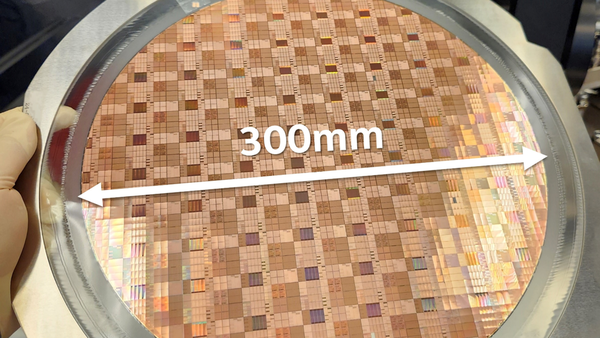
The chiplet reshuffle is spreading beyond logic and memory to power semiconductors. Intel Foundry’s technology research team recently demonstrated GaN chiplet technology based on 300 mm gallium nitride (GaN)-on-silicon wafers for the first time at the 2025 IEEE International Electron Devices Meeting (IEDM). It highlighted the world’s thinnest GaN chiplet, with the underlying silicon substrate only 19 micrometres thick, about one-fifth the thickness of a human hair. It also stressed it secured production-level uniformity on a 300 mm wafer.
A key point is that it integrated a silicon digital control circuit on top of the GaN chiplet in a single process. Previously, power transistors and digital control logic were separated into different chips, causing energy loss during signal exchange and increasing mounting area. Intel’s foundry team said it solved this by implementing a GaN N-channel high-electron-mobility transistor (N-MOSHEMT) and a silicon P-channel metal-oxide-semiconductor (Si PMOS) transistor side by side on the same wafer.
Chips that can be stacked and bonded are emerging as the decisive factor, with the foundry, packaging and IP ecosystem moving as a single set.
The trend is directly linked to discussions about reshaping the value chain. As processes become more advanced, design manpower and costs surge, and gaps emerge that cannot be filled with IP provided by foundries alone. High-speed interface IP such as PCI, USB and HDMI is effectively dominated by a small number of specialist vendors, making it difficult for new entrants to break in.
Ultimately, the industry has little choice but to move as a set, from foundry process selection to building the IP, library and EDA ecosystem. Samsung Electronics said on a conference call held in January that it has a one-stop solution system that provides an integrated offering from semiconductor design and foundry processes to memory and advanced packaging, and that it is holding parallel discussions on products and commercialisation with customers that want it. It said it expects tangible results from a turnkey business model in the medium to long term.
The strategic importance of back-end processes has also increased. SK hynix said it will bolster global integrated manufacturing capabilities across front-end and back-end processes as it prepares an advanced packaging plant in Indiana in the United States. It also saw packaging, testing and quality control as key variables that determine yield and cost. Back-end processes that were handled through outsourcing have effectively been elevated to strategic assets.
After 2-nanometre nodes, competitiveness is expected to hinge on how organically companies can tie together foundry, packaging, interconnect and IP ecosystems across both logic and power semiconductors. An industry official said, "Competition around AI infrastructure demand will play out on a much broader front than a specific process node."
 Dae-geon Seok (석대건)
d2dg@d-today.co.kr
Dae-geon Seok (석대건)
d2dg@d-today.co.kr