KAIST said on Thursday that a research team led by electrical and electronic engineering professor Byungjin Cho (조병진) overcame the limits of higher-density 3D V-NAND memory by applying a new material to a semiconductor layer thinner than a strand of hair. It implemented a "smart door" structure that selectively controls electron movement depending on conditions.
3D V-NAND refers to a memory technology designed to store more information by stacking semiconductor cells vertically. The study is significant because it addressed the slowdown in speed and reliability issues that occur when writing and erasing data, using a new material called boron oxynitride (BON).
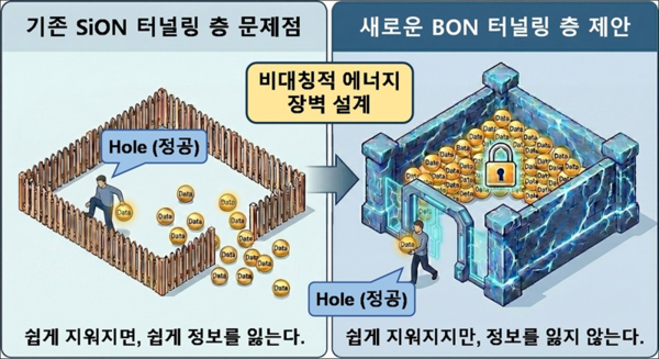
In semiconductor memory, the tunnelling layer, the channel through which data enters and leaves, has struggled to achieve both performance and stability. The tunnelling layer is an insulating layer that serves as an extremely thin channel for electrons to move inside a memory cell.
But with the existing material silicon oxynitride (SiON), a trade-off occurred. If the channel is widened to erase data, stored data leaks out, while narrowing the entrance makes deletion too slow.
KAIST explained that this was the biggest obstacle to implementing next-generation penta-level cell (PLC) technology, which stores 5 bits of information in a single memory cell. PLC stores data by distinguishing 32 voltage states in one memory cell, enabling more information to be stored in memory of the same size.
To solve the problem, the team moved away from silicon-based materials and applied BON, a completely new material, to the tunnelling layer. The material has a distinctive physical property in which the threshold height varies depending on the type of charge.
Using this, the team designed an "asymmetric energy barrier" structure that allows holes, the charge needed to erase data, to pass easily, while preventing electrons, which represent stored data, from leaking out.
An asymmetric energy barrier refers to a structure in which the height of the energy barrier that charges must overcome differs depending on the type of charge. This allows charges to move easily when erasing data while effectively preventing leakage of electrons, which are stored data, to the outside. It works like implementing a "smart door" inside a semiconductor that opens easily when entering but closes tightly when exiting.
Experiments showed devices using a BON tunnelling layer improved data erase speed by up to 23 times versus existing technology. They showed high durability with almost no performance degradation even after tens of thousands of repeated uses. In particular, in penta-level cell operation, which must distinguish 32 fine voltage states, the team succeeded in controlling data distribution between devices with more than 3 times greater precision.
Cho said, "This study is an original technology that can be applied immediately to manufacturing next-generation ultra-high-capacity memory," adding, "It will greatly contribute to maintaining South Korea's technology gap as a semiconductor powerhouse."
The research was led by Dae-hyun Kang (강대현), a combined master's and doctoral student in the electrical and electronic engineering department, as first author, and was presented in December last year at the International Electron Devices Meeting (IEDM), the most authoritative academic conference in the semiconductor field. The study was carried out with support from the Ministry of Science and ICT's National Semiconductor Laboratory Support Core Technology Development Program.