
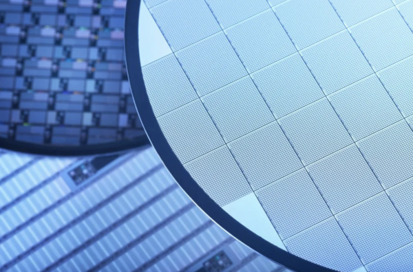
Demand for water infrastructure is expected to expand in tandem with the expansion of semiconductor fabs in South Korea. Whether the required water can be secured at designated sites has emerged as a pre-investment check variable for semiconductor capital expenditure (Capex).
Water use at domestic fabs is already at a level that is hard to compare with other large facilities. According to Kyobo Securities, Samsung Electronics' total global water intake in 2025 was 197.7 million tons, with 90 percent coming from its semiconductor business. SK Hynix used 117.0 million tons. Over the same period, Amazon disclosed 9.5 million tons of direct water intake for its data centres worldwide.
Fab expansion is also planned, and usage is expected to rise further. In June, the government announced three mega projects and presented fab expansions in Yongin and the southwest as investment pillars. Kyobo Securities cited water supply and permits for pipelines as constraints. In South Korea, securing water supply becomes the first hurdle, it said.
As a result, the share of equipment that reuses water inside fabs is increasing. Ultrapure water is the cleanest water used to clean wafers. It must meet a resistivity of 18.2 megaohm-centimetres, close to pure water in theory, and even trace metal ions or fine particles at the level of 1 part per trillion can lead to pattern collapse and device defects. This is why large fabs are adopting advanced water treatment solutions for zero liquid discharge (ZLD), which reuse water by raising used water back to ultrapure grade through reverse osmosis (RO) and ion exchange, lifting reuse rates to more than 90 percent.
Integrated design that ties everything from raw water intake to pretreatment, ultrapure supply, wastewater treatment and reuse into a single system is also spreading. If approached by individual equipment, there are limits to reducing energy and chemical costs, so process and operations need to be designed together to secure stability and economic efficiency at the same time.
Demand increases further as advanced semiconductor processes become more miniaturised. Industry officials said that after the introduction of extreme ultraviolet (EUV) lithography, chemical mechanical polishing (CMP) steps increased as chip structures became more three-dimensional and multilayer metal wiring grew. They said ultrapure water consumption per wafer rose sharply as post-cleaning steps to wash off residue immediately after polishing were frequently added.
Evaporation losses from cooling towers, which cool the heat from EUV equipment that consumes more than 1 to 1.5 megawatts per unit, also account for a large share of fab water use. Demand for waste liquid recycling is also rising as the number of 3D NAND layers climbs to more than 300 and the use of high-purity phosphoric acid for nitride etching increases.
Ultrapure water requirements are spreading beyond fabs to manufacturing processes at partner firms. An official at an ultrapure water equipment company said, "As it has become an era in which equipment makers must prove performance themselves, reaching the customer fab level in their manufacturing processes has become a survival strategy." The official added, "If equipment that has not been precisely cleaned with ultrapure water is shipped to a fab, the equipment itself becomes a source of contamination, inevitably leading to process delays and lower yields."
Global fabs are building reclaimed water facilities first. TSMC supplies 20,000 tons a day by restoring wastewater from the semiconductor industry to ultrapure-grade water at a reclaimed water plant in Tainan, Taiwan, and plans to raise that to 67,000 tons. Samsung Electronics is building pipelines to bring in discharge water from municipal sewage treatment plants and convert it to ultrapure water at fab water treatment facilities.
There is still time before water supply schedules begin. In Yongin, 310,000 tons for phase one of an integrated pipeline is to be supplied in 2031, and 600,000 tons for phase two of the Samsung national industrial complex is due in 2035. There is a gap between the goal of doubling semiconductor production capacity (CAPA) within 5 years and the start of full water supply. As these are government-led projects, the possibility that the supply itself will be cancelled is low, but it could be delayed during talks with local governments and the permitting process, Kyobo Securities analysed.
Kyobo Securities said demand for reclaimed water and ultrapure water infrastructure may also expand during the expansion in Yongin and the southwest. It said water competitiveness will act both as a pre-check variable for semiconductor production capacity and as a factor raising demand across the water infrastructure value chain.
 Daegeon Seok
d2dg@d-today.co.kr
Daegeon Seok
d2dg@d-today.co.kr