Search results for hybrid bonding
Industry
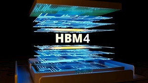
HBM4 thickness rule eased, MR-MUF and TC-NCF upgrade race enters new phase
Competition over sixth-generation high-bandwidth memory HBM4 is shifting after JEDEC eased the HBM package thickness limit to about 775 micrometers from 720. The added margin revives options to refine bump-based processes such as MR-MUF and TC-NCF, potentially delaying hybrid bonding to HBM4E or later. Supply-chain effects are emerging, including Unitest’s contract to supply SK hynix with HBM4 wafer testers worth 22.68 billion won.

Industry
Semiconductor boom, but South Korea\'s chip equipment exports to China fall
South Korea\'s semiconductor exports rose past $40 billion for the first time on a monthly basis, extending a 16-month streak of gains. But exports of semiconductor manufacturing equipment to China edged down in June even as memory chip shipments surged. The article points to China focusing on domestically made back-end processing equipment as the United States tightens controls on advanced lithography tools. Hybrid bonding and other back-end processes are highlighted as key areas of Chinese localisation.
Industry
Applied Materials expands packaging equipment lineup to boost HBM, chiplet yields
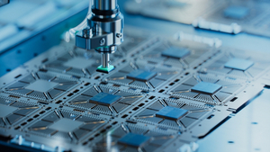
Applied Materials unveiled six new semiconductor manufacturing tools spanning advanced packaging and DRAM processes, the company said on Sunday. It said AI computing faces a “memory wall” as bandwidth and capacity lag growing model sizes and data throughput, driving demand for high-bandwidth memory and 3D stacking. The lineup includes CMP, electrochemical deposition and PECVD systems, two e-beam metrology tools, and an upgraded epitaxy system for DRAM peripheral transistors.
-
Industry
HBM beyond 16 layers brings memory makers\' hybrid bonding shift into view
-
Industry
Justem secures 30 billion won semiconductor policy funding from KDB
-
Industry
Dutch chip equipment maker Besi sees surge in hybrid bonding orders on AI infrastructure investment
-
Industry
Lam Research, Applied Materials consider acquiring Dutch chip equipment maker BESI
-
Industry
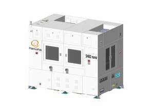
Hanwha Semitec completes development of second-generation hybrid bonder
-

Industry
European semiconductor technology firms turn to South Korea
-

Industry
Korean HBM equipment makers target Japan\'s semiconductor market