Dutch chip equipment maker ASML has started shipping its next-generation high-NA (High Numerical Aperture) EUV lithography tools to chip plants, with each unit costing $400 million, or about 620 billion won.
MIT Technology Review reported on Monday that the tool delivers 8-nanometer (nm) resolution, allowing finer circuits to be etched than with existing EUV systems.
Lithography is the process of shining light onto a silicon wafer to draw transistor and wiring structures. ASML holds about 90 percent of the market for equipment that is effectively essential for producing advanced chips, from smartphone processors to AI server semiconductors. The new tool can draw patterns smaller than the 13 nm possible with existing EUV, and demand is expected to rise among chipmakers seeking higher chip density.
The backdrop is competition in artificial intelligence (AI) infrastructure. OpenAI, Google, Meta and Anthropic are expanding large server farms, driving a surge in demand for chips with higher performance and power efficiency. ASML Chief Technology Officer Marco Pieters (마르코 피터르스) said the explosive expansion now seen in AI becomes possible as customers move to finer processes. He added that what has been seen so far is only the tip of the iceberg.
High-NA EUV does not introduce a new light source. It keeps the existing EUV source but raises the numerical aperture (NA) from 0.33 to 0.55 to etch patterns more precisely. ASML said this can nearly halve transistor size and roughly triple on-chip density. Achieving that requires larger mirrors, a more powerful laser and a faster drive system. A new reticle moves with acceleration of up to 22g, and Germany's Zeiss designed a larger reflector and a new 12-ton projection system.
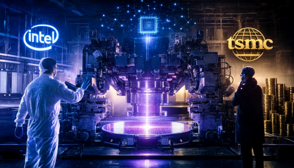
Intel is the leading early customer. Intel brought in its first high-NA tool to its Oregon plant in the spring of 2024 and has been assembling and testing it. Intel fellow Mark Phillips (마크 필립스) expressed satisfaction, saying the system's condition is stabilising quickly. Intel plans to deploy the tool first in some precision processes and then gradually broaden its use. TSMC, by contrast, says it will adopt high-NA EUV when the technology is mature enough to deliver the maximum benefit to customers. The industry expects TSMC to hold out as long as possible with existing EUV and multipatterning before making a full shift in the 2030s.
Cost will be a factor that determines the pace of adoption. Existing EUV tools already cost well above $100 million, or about 154.06 billion won, but high-NA EUV is far more expensive at about $400 million. Even if the benefits of simplified processes and better performance are clear, chipmakers face a heavy burden in rapidly expanding use across large-scale mass-production lines. Semianalysis researcher Jeff Koch (제프 코크) said performance improves by about 30 to 50 percent, but the tool could be the first among ASML's products whose business case is not immediately clear.
Regulation is also splitting the market. The United States pressured the Dutch government in 2019 to prevent ASML from selling advanced equipment to Chinese companies. As a result, China has not secured high-NA or even existing EUV tools and has chosen a strategy of pushing deep ultraviolet (DUV) lithography and multipatterning as far as possible. David Lin (데이비드 린), a senior adviser at the Special Competitive Studies Project, said China will push DUV to its limits. China is also trying to offset a shortage of high-performance AI chips through software by developing lightweight large language models such as DeepSeek.
Efforts to shake ASML's dominance are also continuing. U.S. startup Substrate is developing lithography equipment that uses X-rays made with particle accelerators and has set a goal of mass production by 2030. Norway's Lase Lithography is pursuing a method that uses an energy-driven helium atom beam instead of light. Both companies, however, are assessed as needing to bridge the gap between the laboratory stage and mass production.
ASML is also preparing for what comes after high-NA. It is reviewing "hyper-NA" that raises the numerical aperture to 0.75 and studying ways to push resolution down to about 6 nanometers. ASML vice president for technology Jos Benschop (요스 벤스호프) said no practical alternative is visible so far and that there is no serious competitor in the mass production of leading-edge chips. The next competition in the semiconductor industry depends on who can connect this equipment to stable mass production first.