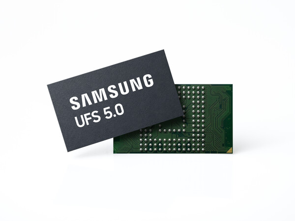
As on-device AI that runs directly on mobile devices spreads, competition to improve storage performance is accelerating. Samsung Electronics said on Monday it has developed the industry's first UFS 5.0, the latest Universal Flash Storage standard from semiconductor standards body JEDEC.
The product is designed based on Samsung’s ninth-generation V-NAND. It supports sequential read speeds of 10.8 GB/s and sequential write speeds of 9.5 GB/s. That is about double UFS 4.1 for both reading and writing.
Power efficiency has also improved. Samsung newly applied clock-gating technology that blocks operating signals for unused circuits and multi-voltage technology that reduces power consumption by applying optimal voltages by circuit. The company said this boosts power efficiency by more than 40 percent versus UFS 4.1.
The package measures 7.5 mm wide, 13 mm long and 0.9 mm high. It is 16.7 percent smaller than the previous model. It offers up to 1 TB of capacity, and the company said it increased design flexibility so it can be used not only in smartphones but also in XR extended reality headsets and AI wearables.
Samsung will start mass production of UFS 5.0 from the fourth quarter of this year. It plans to expand supply from flagship smartphones to next-generation devices such as XR headsets and AI wearables.
Jangseok Choi (최장석), head of the product planning team at Samsung’s memory business, said: "In the era of on-device AI, storage is becoming a key element that determines the AI experience, beyond being a simple data storage space. Through completing development of the industry’s first UFS 5.0, Samsung Electronics will present a new standard for next-generation mobile storage and continue to lead AI mobile innovation."