SemiFive and ICY Tech said on May 7 they succeeded in taping out an edge AI semiconductor based on Samsung Foundry's 8-nanometre eMRAM technology. The tape-out is the first case in Asia in which 8-nanometre eMRAM technology is introduced into a commercial product. It is also SemiFive's first eMRAM-based ASIC design project, with SemiFive responsible for implementing production-ready silicon. Samsung Foundry's 8LPU process was applied.
MRAM, or magnetic random access memory, stores data through resistance changes in an MTJ, or magnetic tunnel junction, device. Because it does not store electric charge like DRAM, data is retained even when power is turned off, and periodic refresh operations are not needed. It is assessed as a key technology for AI semiconductors and low-power edge devices because its write speed is more than 1,000 times faster than flash memory and power consumption is lower. eMRAM is embedded memory that integrates such MRAM inside system semiconductors such as SoCs and MCUs, and is drawing attention as an on-chip memory solution that will replace embedded flash, or eFlash.
In the project, the two companies combined ICY Tech's PNM, or processing near memory, technology with SemiFive's SoC design platform. The key is that they built an architecture that can perform AI computing in edge environments without a separate network connection. It can process models of up to 2 billion parameters on-device, delivering performance at a level that enables real AI use such as text summarisation, translation and conversational reasoning. This is an area that existing SRAM-based edge AI chips have found difficult to implement due to die area and power limits.
ICY Tech, founded based on the Center for Applied Magnetics in the Department of Physics at Peking University, has developed MRAM technology specialised for AI inference based on expertise in magnetics and spintronics. It has capabilities including MRAM bitcell and peripheral circuit design, high-bandwidth readout and in-situ matrix-vector multiplication, or GEMV, implementation. SemiFive, a key design solution partner in Samsung Foundry's SAFE ecosystem, has carried out ASIC projects ranging from AI and HPC to edge AI.
The architecture developed this time targets edge devices that operate in offline environments, such as AI PCs, private AI agents and humanoid robots. It is expected to be applied in various fields including robotics, or physical AI, automotive semiconductors for autonomous driving and cockpits, and smart devices.
Yves Zhu (이브 주), CEO of ICY Tech, said, "This collaboration is a challenging project to implement a spintronics-based AI inference architecture in silicon on Samsung Foundry's 8-nanometre (8LPU) process." He said, "By applying eMRAM's ultra-low-power and non-volatile characteristics to an AI accelerator, it will become a new milestone for edge AI semiconductors." Zhu added, "I am confident it will prove performance that goes beyond the limits of existing architectures in the global AI inference market and can redefine the standard for power efficiency."
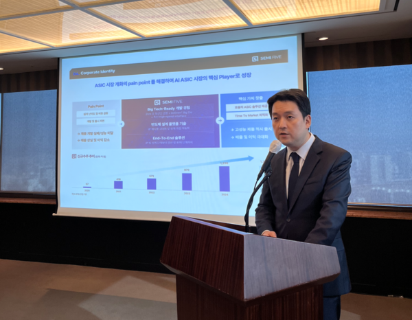
Myung-hyun Cho (조명현), CEO of SemiFive, said, "As ASIC design in new areas using next-generation memory such as eMRAM gains momentum, the role of an AI ASIC design specialist partner that takes responsibility for the entire process will inevitably grow." He added, "This cooperation with ICY Tech is meaningful in that we have expanded our portfolio into a new design area called MRAM."