As memory chip manufacturing processes become longer and more precise, wafer carriers known as FOUPs have emerged as a key factor affecting yields. With wafers staying inside fabs for more than 100 days, the importance of contamination control has also grown. Orders for FOUP cleaning and humidity-control equipment from South Korean toolmakers are surging.
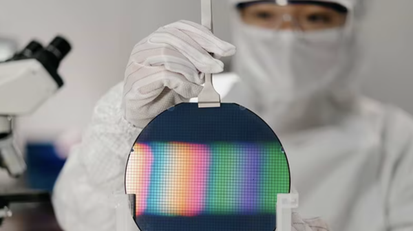
The strategic value of FOUPs, semiconductor wafer carriers, has risen sharply, the industry said on Feb. 24. A FOUP is a carrier that holds 25 wafers and moves them between process tools. It may look like a simple plastic container, but failure to control contamination inside a FOUP can hurt yields and even lead to situations where equipment worth hundreds of billions of won comes to a stop.
Advanced chips such as high-bandwidth memory (HBM) have more process steps, and wafers increasingly stay inside fabs for more than 100 days, the industry said. The cycle time for a 28-nanometre process was about 40 days, but it has risen to more than 100 days for 5-nanometre and 3-nanometre processes. HBM also adds through-silicon via (TSV) and stacking steps, extending dwell time further. That means wafers spend more than 70 percent of the overall manufacturing cycle waiting inside FOUPs.
The problem is that the longer wafers remain in FOUPs, the greater the contamination risk. If humidity inside a FOUP is high, an oxide film can form on the wafer surface, and gas particles generated by processed wafers can affect other wafers. This is called AMC, or airborne molecular contamination, and in processes below 10 nanometres, even nanometre-level contamination can be fatal to yields. If FOUP contamination is found, cleaning or replacing the carrier can force expensive tools such as EUV lithography systems, worth hundreds of billions of won, to halt and wait.
As a result, technology to control the environment inside FOUPs has emerged as critical. A FOUP is not just a carrier but, in effect, a mobile cleanroom that determines wafer quality. How precisely humidity and contamination are managed is directly linked to yields. That is why chipmakers are moving to secure FOUP cleaning and humidity-control equipment.
Orders are also being reported for FOUP-related equipment and parts. ISTE said on Feb. 20 it won an additional order from SK hynix for FOUP cleaners. The order will be applied to a new fab in Cheongju and the Icheon fab. ISTE said cumulative order intake from January to the present has risen by more than 300 percent from the same period a year earlier. An ISTE official explained, "As HBM and DDR5 DRAM production expansion is being pursued, we are responding to equipment demand spanning new fabs and existing fabs."
Demand is also rising for solutions that manage conditions inside FOUPs. Justem provides a first-generation solution called N2 Purge that injects nitrogen into FOUPs to lower humidity from 45 percent to 5 percent. As processes become finer, even 5 percent humidity has become insufficient. Justem's second-generation solution, JFS, applies vertical laminar-flow control technology to reduce humidity to below 1 percent. It blocks high-humidity airflow entering FOUPs from EFEM, a wafer transfer system. The industry said the company supplied the solution to all three major memory makers: Samsung Electronics, SK hynix and Micron.
HBM capacity surge also lifts demand for backend equipment parts
As the three memory makers sharply increase HBM capacity and continue investing in backend facilities, the FOUP-related market is expected to draw more attention. Daishin Securities said the three DRAM makers' HBM capacity is expected to expand to 360,000 wafers per month by the end of 2025, 495,000 wafers per month by the end of 2026 and 580,000 wafers per month by the end of 2027. It cited the impact of a full-scale ramp-up of HBM4, where securing yields is difficult.
In response, chipmakers are expanding backend investment. SK hynix will build a next-generation advanced packaging plant in Cheongju spanning 70,000 pyeong, known as the P&T Plant 7. It will invest a total of 19 trillion won, targeting completion by the end of 2027. It is also building an advanced packaging plant for AI memory in Indiana, investing about $3.87 billion, with mass production targeted for the second half of 2028. Micron is also building a new backend plant in Singapore with a $7 billion investment and will begin full operations from 2027.
As backend expansion accelerates, the importance of process-environment management solutions such as FOUP cleaning and humidity-control equipment is expected to grow further. Daishin Securities said, "Amid expanding HBM penetration, a shortage of backend fab space will intensify," adding, "It is necessary to pay attention to backend equipment and OSAT."