The keyword that will decide the future of semiconductors is "yield". Semicon Korea 2026 set a record with 550 companies and 75,000 participants. On the floor, interest was especially high in metrology and inspection (MI) equipment companies ahead of mass production of HBM4 and a 2-nanometre process.
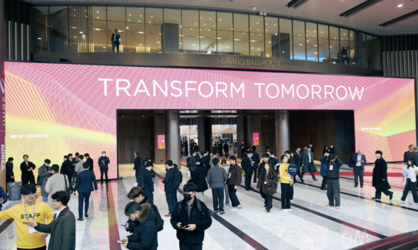
Semicon Korea 2026 has been held at Seoul's COEX since Feb. 11. It is being held on a record scale, with about 550 companies, more than 2,400 booths and 75,000 pre-registered visitors.
The key agenda running through this year's event was "yield". As demand for AI semiconductors moves into HBM4, a sixth-generation high-bandwidth memory, and a 2-nanometre process, making chips properly has become more important than simply making them. As a result, booths for MI equipment makers that catch unseen defects were especially crowded.
The problem is that as processes stack vertically and get finer, catching defects becomes exponentially harder. An equipment industry official met at the venue explained, "HBM stacks chips into 12 layers and 16 layers, but tiny voids (empty spaces) or bonding defects that occur between them cannot be found with existing optical inspection," adding, "things that were sufficient with sampling inspection in the past are now being required to undergo full inspection."
"Technology inflection point" was also a key topic in the keynote speeches. Lee Seong-hun (이성훈), vice president of R&D process at SK Hynix, who delivered a keynote speech that day, said, "The memory industry has reached a technology inflection point." He stressed, "As the limits of DRAM scaling become visible and NAND shifts to ultra-high-layer stacking, another technology inflection point is expected after 2027," adding, "we cannot maintain the development cadence with past methods."
Lee presented "AI-based R&D innovation" as a solution. He said, "If we use AI models, we can evaluate a wider range of materials in a much shorter time than existing methods, and we can find optimal process conditions with fewer experiments," adding, "we must shift from 'man-month' based R&D that relies on adding personnel to AI-based R&D that maximises time efficiency." SK Hynix also disclosed a case in which it worked with Nvidia to optimise process simulation.
Song Jae-hyuk (송재혁), president and chief technology officer at Samsung Electronics, also said, "HBM4 quality has already reached the highest level," adding, "we are also preparing manufacturing of next-generation form factors such as 'Z-HBM', which stacks into a 3D structure beyond vertical stacking," showing confidence.
MI equipment demand surges..."Semiconductor inspection system market $15.78 billion in 2035"
According to global market research firm Research Nester, the semiconductor inspection system market is expected to grow at an average annual rate of more than 8 percent from 2026 to 2035 and exceed $15.78 billion in 2035. The World Semiconductor Trade Statistics (WSTS) forecast the global semiconductor market will grow more than 25 percent from a year earlier this year to about $975.0 billion.
Equipment makers from South Korea and abroad deployed a full range of next-generation inspection and metrology technologies at this exhibition. Teraview introduced a non-destructive inspection system, "EOTPR", using terahertz waves (THz) and highlighted its ability to detect tiny defects inside stacked structures. EVG showcased a die-to-wafer (D2W) overlay metrology system along with hybrid and fusion bonding solutions. Justem unveiled its "JDS" solution that controls humidity and temperature of EFEM and FOUP at the same time and stressed technology to secure yield in fine processes. ISTE displayed a diversified lineup including a FOUP inspection combined device and PECVD equipment.
The industry believes that investment in inspection and metrology equipment has become a necessity rather than a choice, as a very small difference in yield can create performance gaps worth hundreds of billions of won. An industry official said demand for MI equipment will keep rising until HBM4 and 2-nanometre processes enter full-scale mass production.