As AI semiconductor chips become larger, limits of existing plastic PCB substrates are coming into focus. Heat-induced warpage becomes more severe as chips grow. A material aiming at this gap is glass substrates.
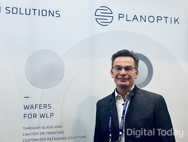
German glass-substrate specialist Planoptik AG has begun targeting the South Korean market. Carsten Wesselkamp (카르스텐 베셀캄프), Planoptik vice president of sales, visited South Korea through the EU Business Hub programme to coincide with Semicon Korea 2026. "As demand for glass cores has increased, we decided to expand the business," Wesselkamp said. "We already have long experience in glass processing, so entering the semiconductor packaging market was natural," he said.
Planoptik has built up optical glass processing technology for 54 years. From 2000, it entered substrate manufacturing for semiconductors and MEMS sensors. Glass was suitable as an insulating material needed for sensor production because of its heat resistance and long-term stability.
Glass substrates in particular operate stably even in harsh environments in semiconductor processes. "In the semiconductor or PCB industry, many chemicals are used, and not all substrate materials can withstand them," Wesselkamp said. "Glass is resistant to almost all process chemicals, so it is suitable for harsh process environments," he added.
The difference from plastic substrates is also clear. Plastic can deform due to heat and its physical properties can change over time. Glass, by contrast, retains its shape at temperatures of about 500 degrees and its physical properties do not change for 10 to 20 years. "Glass has strengths in applications that require long-term stability," Wesselkamp said.
Insulation properties of glass substrates are also coming into focus in an era of high-frequency communications. "If conductive materials such as silicon are used as core substrates, parasitic capacitance occurs on top of thin insulation layers," Wesselkamp said. "After 5G, as it moves to 6G and 7G, using conductive materials will become almost impossible," he added. He said glass is free from this issue because it is an insulator.
Even so, it will take time before full-scale mass production of glass substrates. He said a shift would soon occur in a significant number of areas. "The process of processing glass into substrates is new and more complex than existing materials," Wesselkamp said. "But if the advantages of using glass are large enough, it will quickly enter mass production and replace other materials," he added.
Planoptik already has South Korean customers from 15 years ago. It currently supplies items such as carriers for thin-wafer handling. "South Korea has many automakers, and cars need sensors," Wesselkamp said. "Supplying materials to companies that produce sensor substrates is the core strategy for expanding in the South Korean market," he said. "We mass-produce wafers for the sensor systems market in Europe and Taiwan," he added. "We plan to actively target the South Korean market based on our existing product line."