
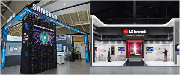
Samsung Electro-Mechanics and LG Innotek are unveiling new semiconductor package substrate technologies. Samsung Electro-Mechanics said on Sept. 9 it will take part in KPCA Show 2026, held at Songdo Convensia in Incheon from Sept. 9 to 11, to showcase next-generation semiconductor package substrate technology. LG Innotek is also participating in the event at the same venue over the same period and is exhibiting next-generation substrate technologies and products.
Semiconductor package substrates are key components that connect high-density chips to the mainboard, delivering electrical signals and power. As performance of AI accelerators and server CPUs improves rapidly, package substrates are shifting from simple connecting parts to technologies that determine performance, power efficiency and signal stability. AI semiconductors that integrate multiple high-performance chips into a single package require advanced technologies such as large-area and high-layer designs, fine circuits, and micro vias and bumps.
Samsung Electro-Mechanics is exhibiting five items at the show: 2.5D package substrates, 2.1D package substrates, glass substrates, automotive FCBGA and UTCSP, an ultra-thin semiconductor package substrate. Key technologies include 2.1D substrates that enable direct chip-to-chip connections without a silicon interposer and 2.5D substrate technology that reduces warpage in large-area, high-layer substrates. It is also showcasing high value-added substrates with expanded applications from data centres to mobile and autonomous driving.
LG Innotek is unveiling an FC-BGA for AI accelerators for the first time at the exhibition. The large-area substrate has a side length exceeding 100 mm and incorporates high circuit density and ultra-fine circuit implementation technology. The company set a goal of mass-producing high value-added FC-BGA for AI training and inference, including this product, in 2027. It is also exhibiting chip-embedding technology that places chips inside the substrate to minimise connection distance, and Cu-Post, a copper-pillar process used for communications semiconductor substrates.
Both companies are also accelerating development of glass substrates. Using glass as a core material reduces substrate warpage and secures signal and power efficiency, and Samsung Electro-Mechanics is introducing a key process that drills microscopic channels in glass material and fills them with metal. LG Innotek set a target of mass-producing glass substrates in 2028.
Joo Hyuk (주혁), a vice president at Samsung Electro-Mechanics and head of its Package Solution Business Division, said, "As the high-performance semiconductor market grows in areas such as AI accelerators, servers and autonomous driving, the role of package substrates and the level of technical difficulty are also rising rapidly." He added, "We will respond to the high-end semiconductor package substrate market by advancing large-area, high-layer and ultra-fine circuit technologies and next-generation packaging technologies."
Cho Ji-tae (조지태), head of LG Innotek's Package Solution Business Division and an executive vice president, said, "This exhibition will allow people to see how LG Innotek's substrates can be used across various industries such as AI, smartphones and mobility." He added, "We will change the paradigm of the substrate market with innovative products."
 Daegeon Seok
d2dg@d-today.co.kr
Daegeon Seok
d2dg@d-today.co.kr