Search results for Siemens EDA
Industry
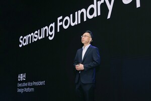
Samsung Electronics unveils 2 nm and SRAM roadmap at SAFE Forum
Samsung Electronics said it is expanding cooperation with domestic and overseas partners to broaden the AI semiconductor ecosystem. It held SAFE Forum 2026 in Seoul and presented its next-generation foundry technology strategy and plans to expand ecosystem cooperation. About 400 people attended, with 21 partners showcasing solutions. Samsung also unveiled a DTCO strategy, a next-generation 2 nm process and plans to strengthen SRAM competitiveness, while joining initiatives such as M.AX and K-CHIPS.
Industry
Intel pushes into foundry market, focus on Samsung response
Intel’s push into the contract chipmaking market is becoming visible through orders from big tech firms, with Tesla set to use Intel’s 14A process for AI chips and Google reportedly shifting part of TPU production. The move comes as TSMC capacity constraints have opened space for alternatives such as Samsung Electronics. Intel’s U.S. government backing and leadership hires add to competition for U.S. customer volumes, as Samsung prepares to outline its technology strategy at upcoming forums in Seoul.
Industry
China\'s EDA industry joins Huawei\'s Tau Scaling 3D chip push; commercialisation seen 4 to 5 years away
China\'s semiconductor design software industry is moving to support Huawei\'s next-generation chip strategy, with companies developing tools aligned to its Tau Scaling framework and 3D design approach. Empyrean Technology unveiled a 3D IC verification platform, while a Peking University team showed a prototype compatible with Huawei\'s Logic Folding architecture. Industry and research groups say technical hurdles and gaps with U.S.-led full-flow EDA suites mean commercialisation could take 4 to 5 years.