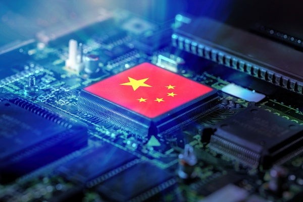
China's semiconductor design software (EDA) industry is increasingly stepping up to support Huawei's next-generation chip development strategy. Still, it is expected to take significant time to catch up with the global EDA market dominated by U.S. companies.
The Hong Kong-based South China Morning Post (SCMP) reported on June 12 that major Chinese EDA companies have recently started full-scale technology development tailored to Tau Scaling, a new semiconductor design framework proposed by Huawei.
Most recently, Chinese EDA company Empyrean Technology unveiled Argus, a physical verification platform for three-dimensional integrated circuit (3D IC) design. The company explained that 3D IC technology is a key means of implementing Huawei's Tau Scaling strategy.
Earlier, a Peking University research team also showcased a prototype EDA product for 3D design compatible with Huawei's Logic Folding architecture. The move came shortly after Huawei announced its Tau Scaling framework last month.
At the core of Tau Scaling is shifting the benchmark for improving semiconductor performance from transistor miniaturisation to reducing signal travel time within a system. Huawei presented a plan to use Logic Folding technology, which stacks planar circuits vertically, to achieve leading-process levels of density and performance without advanced EUV lithography equipment. This is interpreted as an attempt to find a new workaround as U.S. semiconductor sanctions restrict access to advanced equipment.
China's semiconductor industry is rushing to develop related design tools in line with the strategy, but it believes commercialisation will take considerable time.
Han Chaoyang (한차오양), vice president of marketing at Chinese AI chip company ListenAI, said, "To apply Tau Scaling to actual industry, China needs to secure its own EDA design and simulation tools." He said it is not a problem Huawei can solve alone and requires cooperation across China's entire semiconductor supply chain.
The technical difficulty is also substantial. Chinese semiconductor research firm ICwise pointed out that most existing EDA tools are built on the premise of two-dimensional planar design. By contrast, 3D semiconductor design requires new technical challenges such as multilayer placement and routing, interlayer power integrity analysis, and complex timing verification.
ICwise forecast that not only China but also global research teams are still in the early stages in this field, and that at least 4 to 5 years will be needed to achieve engineering implementation at a level suitable for mass production.
Still, the market expects Huawei's new strategy to offer new growth opportunities for China's EDA industry. Wu Mingyuan (우밍위안), an analyst at Huachuang Securities, said China's EDA industry can move beyond simply filling gaps left by overseas products and into a collaborative innovation stage optimised for Chinese processes and systems.
He said companies with capabilities in process collaboration, manufacturing data acquisition and customer ecosystems are likely to benefit. He named Empyrean Technology, Primarius Technologies and Semitronix as key beneficiaries.
Still, the gap with U.S. companies remains large. The global EDA market is effectively dominated by Synopsys, Cadence Design Systems and Siemens EDA. Chinese companies are competitive in individual design domains, but are seen as still lacking integrated full-flow solutions that support the entire semiconductor development process.
Semiconductor analysis firm SemiAnalysis said, "Because software complexity has no physical limits, building a competitive EDA ecosystem is as difficult as developing advanced processes."
In fact, the combined revenue of China's three listed EDA companies last year was about $308 million, only about 1.8 percent of the global market. China's share of the EDA market has still expanded from 0.9 percent in 2018 to 5.3 percent in 2024, showing steady growth.
The industry sees Huawei's Tau Scaling strategy as capable of opening new opportunities for China's EDA industry, but believes it will not be easy to replace in a short time the integrated ecosystem built by U.S. companies.
Ultimately, analysts say the success or failure of China's EDA industry depends on how quickly it can apply Huawei-style 3D design structures to actual mass-production environments, and whether it can build an integrated design ecosystem to compete with Synopsys and Cadence.