Samsung Electronics is expanding cooperation with domestic and overseas partners to broaden the artificial intelligence semiconductor ecosystem. Samsung Electronics held SAFE Forum 2026, its foundry ecosystem programme, at its Seocho office building in Seoul on Tuesday and unveiled its next-generation foundry technology strategy and plans to expand ecosystem cooperation.
About 400 people from customers and partners attended the forum. In five areas including EDA software that automates chip design and IP blocks that reduce circuit design time, 21 partners set up booths and introduced solutions that support Samsung Electronics foundry customers. Speakers including AI chip fabless company Rebellions and EDA company Siemens EDA presented examples of semiconductor development using Samsung Electronics' foundry processes and ways to support 2.5D and 3D chip design.
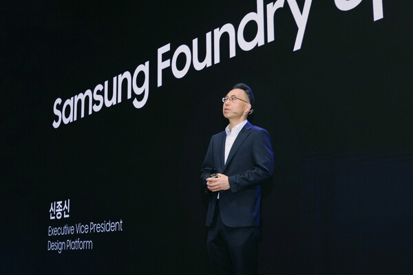
In a keynote speech, Shin Jong-shin (신종신), head of the design platform development group at Samsung Electronics' foundry business, said: "Samsung Electronics will raise its capabilities to respond to AI demand while actively communicating with customers and partners by using the SAFE Forum." He said: "We are stepping up cooperation with global AI and HPC customers and also strengthening cooperation with domestic system semiconductor customers. We will strengthen our role as a domestic system semiconductor industry platform beyond foundry production."
Park Sung-hyun (박성현), CEO of AI chip fabless company Rebellions, said: "We developed the 'Rebel-100' NPU based on Samsung Electronics' 4-nanometre foundry process and advanced packaging." He said: "We will cooperate in the AI semiconductor area and build sovereign AI."
An NPU is a neural processing unit designed to mimic the human brain. Gene Marie Brunet, senior vice president at Siemens EDA, said: "In 2.5D and 3D heterogeneous chip integration, broad support in yield, design verification, reliability and packaging is essential." He said: "Siemens EDA will support customers so they can quickly realise AI and HPC semiconductors using Samsung's leading-edge processes."
Samsung Electronics also unveiled a process innovation roadmap optimised for AI semiconductors, including a DTCO strategy that simultaneously optimises design and process technology to improve power, performance, area, yield and manufacturing costs, a next-generation 2-nanometre process and plans to strengthen SRAM technology competitiveness.
SRAM is volatile memory that retains data only while power is supplied. It is known for fast processing speed but difficulty in scaling to large capacity. Samsung Electronics said it is supporting development of next-generation products demanded by AI semiconductor customers through this.
Samsung Electronics is developing low-power, high-performance on-device AI semiconductors needed for the automotive, home appliance, robotics and defence industries by participating in M.AX, a manufacturing AI transition alliance promoted by the Ministry of Trade, Industry and Energy. It is also reducing the early development burden for domestic fabless companies through its MPW programme, which produces and verifies multiple semiconductor products on a single wafer. The company said it is also participating in the K-CHIPS project, operated by the Ministry of Trade, Industry and Energy, the Korea Institute for Advancement of Technology and the Korea Semiconductor Industry Association, and contributing to next-generation semiconductor research and development and workforce training.