Search results for PECVD
Industry
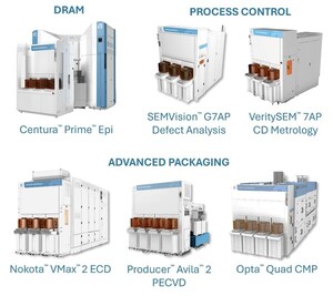
Applied Materials expands packaging equipment lineup to boost HBM, chiplet yields
Applied Materials unveiled six new semiconductor manufacturing tools spanning advanced packaging and DRAM processes, the company said on Sunday. It said AI computing faces a “memory wall” as bandwidth and capacity lag growing model sizes and data throughput, driving demand for high-bandwidth memory and 3D stacking. The lineup includes CMP, electrochemical deposition and PECVD systems, two e-beam metrology tools, and an upgraded epitaxy system for DRAM peripheral transistors.
Industry
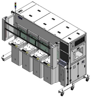
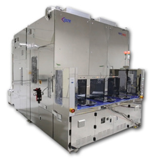
Applied Materials unveils two deposition systems for sub-2 nm GAA processes
Applied Materials on Monday unveiled two deposition systems tailored for sub-2 nanometre gate-all-around (GAA) transistor processes. The company said GAA transistor fabrication requires more than 500 process steps to build internal 3D structures, with many steps demanding near-atomic tolerances. One system uses selective bottom-up silicon nitride deposition to protect shallow trench isolation structures and reduce parasitic capacitance. The other controls metal gate stacks with atomic-level uniformity and integrates multiple metal deposition steps on one platform.
Industry
Yield takes center stage at Semicon Korea 2026
Yield emerged as the key theme at Semicon Korea 2026, held at Seoul\'s COEX from Feb. 11, as the event drew 550 companies and 75,000 pre-registered visitors. With HBM4 and 2-nanometre processes approaching mass production, interest has surged in metrology and inspection equipment to detect hidden defects. SK Hynix executives flagged a technology inflection point and urged AI-based R&D. Equipment makers showcased next-generation inspection and bonding technologies.