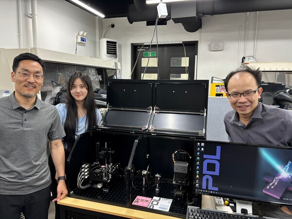
KAIST and IBM have developed a measurement technique that can find internal defects in semiconductors with 1,000 times greater precision. KAIST said on Thursday that a joint team led by Professor Byeongha Shin of its Department of Materials Science and Engineering and Oki Gunawan of IBM's T.J. Watson Research Center developed a method to simultaneously analyse internal semiconductor defects and electron transport characteristics.
The technique combines Hall measurements with light and temperature conditions. Semiconductors contain defects called electron traps, which capture electrons and block their movement. When electrons are caught in traps, leakage current can occur or performance can deteriorate. Identifying the density of electron traps and the strength of electron capture is essential for evaluating semiconductor performance.
The team added light exposure and temperature variation conditions to conventional Hall measurements. Hall measurements analyse electron movement using electric and magnetic fields. When light is shone weakly, newly generated electrons are captured first by electron traps. When light intensity increases, the traps become saturated and electrons generated afterward move freely.
The team analysed this change process and calculated the amount and characteristics of electron traps. A single measurement can now yield electron mobility, lifetime, travel distance and trap characteristics at the same time. Existing methods required multiple separate measurements.
The team applied the technique to silicon semiconductors and succeeded in verifying its accuracy. It then applied the method to perovskite, a next-generation solar cell material, and found trace amounts of electron traps that were difficult to detect with existing methods. Measurement sensitivity improved by about 1,000 times compared with existing technology, it said.
Byeongha Shin said the research presented a new method that can simultaneously analyse the flow of electricity in semiconductors and factors that interfere with it in a single measurement. He said it would become an important tool for improving the performance and reliability of various semiconductor devices, including memory semiconductors and solar cells.
The research results were published on Jan. 1 in the international academic journal Science Advances, with doctoral student Chaeyeon Kim of the Department of Materials Science and Engineering as first author.