Semiconductor equipment makers are moving to strengthen their “test chip” capabilities. Unlike the past, when deliveries of tools were the end of the process, the era of ultra-fine manufacturing now requires equipment makers to process wafers themselves and prove performance to win orders. As the opportunity cost of production lines rises, foundry and memory makers have become reluctant to run tests on their own equipment. The need to prove performance is strengthening the testing stage.
The dynamics of the semiconductor value chain are changing. In the past, chipmakers presented specifications to equipment makers, which then developed tools to meet them and delivered the equipment. But that approach no longer works for ultra-fine processes of 2 nanometres or below. Losses are too large to stop mass-production lines that use extreme ultraviolet (EUV) lithography tools and advanced deposition and etching equipment to test new tools or materials. Chipmakers, increasingly unable to accept risks such as wafer losses and lower line utilisation, have begun demanding validated solutions from equipment makers.
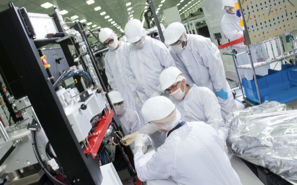
Applied Materials (AMAT) is expanding investment in a dedicated test chip organisation and R&D infrastructure in response to the shift. Michael Chudzik (마이클 추지크), AMAT corporate vice president and general manager of Semiconductor Technology, said at a media briefing on Feb. 12, “We have dedicated personnel for test chip design.” He added, “We make test chips with the same dimensions as customer products and use them when developing new processes.” He added that validation must be completed at the test chip stage to give customers confidence.
AMAT has built a “META Center” in New York state and secured access to EUV lithography tools. Chudzik said, “Thanks to the META Center, we can use the latest EUV lithography capabilities.” He added, “This allows us to make test structures similar to an actual mass-production environment.” AMAT is also pursuing global infrastructure investment including the EPIC Center in Silicon Valley and its Korea research lab. The fact that an equipment maker is building its own EUV-class test environment marks a departure from the past.
Foundries are also stepping up test chip collaboration with equipment makers. Samsung Electronics is developing a second-generation 2-nanometre process with a goal of mass production in the second half of this year. Samsung Electronics said on its fourth-quarter earnings conference call, “We are currently conducting PPA evaluations for product design and test chip collaboration in parallel with major customers.” It added, “Technology verification in the pre-mass production stage is also progressing as planned.” That indicates a structure is taking hold in which foundries work closely with equipment makers, as well as customers, at the test chip stage.
◆ Semiconductor equipment makers: “Test chips are a means to be adopted by customers”
The growing importance of test chips is rooted in the complexity of 3D structures. 3D NAND is now stacked at more than 300 layers, and Samsung Electronics has previously presented a roadmap extending to 1,000 layers. As stacks deepen, a key challenge is uniformly depositing thin films in narrow, deep holes, known as high aspect ratio structures. The problem is that verifying this uniformity itself is very difficult.
The existing method is cross-sectional analysis using a transmission electron microscope (TEM). It involves cutting an extremely small sample from a wafer using ion milling and examining it under a microscope, requiring nanometre-level precision and taking a long time. According to the industry, this method can analyse only around 7 samples per day.
By contrast, using dedicated test chips can cut analysis time to about 3 minutes, making it possible to measure hundreds of samples per day. As the pace of process tuning accelerates in the mass-production ramp-up stage, the timing of yield improvement can also be brought forward.
Equipment makers are focusing on test chips ultimately to drive “customer adoption”. As ultra-fine processes expand, competition in test infrastructure is expected to intensify. At 2 nanometres and below, losses from halting mass-production lines grow exponentially, leaving chipmakers with little choice but to demand pre-validation from equipment makers. For equipment makers as well, securing EUV-class test capabilities is becoming a condition for survival, because they can fall behind in order competition without their own test infrastructure.
Chudzik said, “After the test chip stage, we run learning tools or carry out demonstrations in the customer’s fab.” He added, “The ultimate goal is to operate on the customer wafer, and that is how the tool is adopted.” He added, “The performance metric is tool adoption, and test chips are a means to reach that goal.”