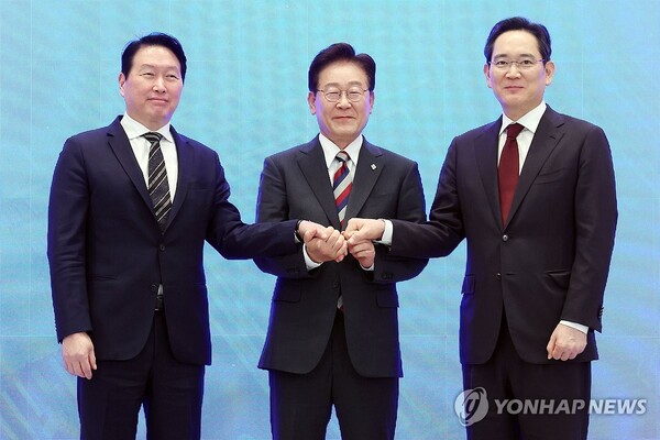
Samsung Electronics and SK Hynix on Wednesday unveiled large-scale investment plans for the Chungcheong region. Samsung plans about 140 trillion won and SK Hynix 100 trillion won, bringing the total investment announced by the two companies to 240 trillion won. SK Hynix, in particular, is pushing to expand NAND flash capacity amid supply shortages, making its response to memory supply and demand one pillar of the investment.
The two companies announced their plans at a public report meeting on a vision for advanced industry development in the Chungcheong region, held at Samsung Display’s Asan campus in Asan, South Chungcheong Province. Samsung aims to develop Chungcheong into a materials and components hub, while SK Hynix wants to build Cheongju into a core base for memory semiconductors. Domestic investment in key businesses such as semiconductors, batteries and displays has been concentrated in a specific region.
Samsung said it will invest about 140 trillion won, focusing on what it called future growth engines: cutting-edge displays, high-bandwidth memory (HBM) fabs, next-generation batteries and package substrates for AI servers. It aims to build Chungcheong into a global base for materials and components and create 250,000 jobs.
Investment targets will be split by affiliate. Samsung Electronics will invest in 5 HBM fab lines in Onyang and expand and modernise HBM-related equipment in Cheonan. Samsung Display will expand high value-added OLED lines in Asan for smartphones and IT, XR and automotive, and humanoid and wearable devices. Samsung SDI will build a mother line in Cheonan to validate next-generation battery technology and lay the groundwork to spread proven technology globally. Samsung Electro-Mechanics will expand facilities in Sejong for AI server package substrates and pursue core technology research and development and talent development.
SK Hynix will invest 100 trillion won in Cheongju alone. Kwak Noh-jung (곽노정), chief executive officer of SK Hynix, said, "We plan to invest 80 trillion won in M17, which will produce NAND, and 20 trillion won in P&T7 and other facilities to strengthen advanced packaging." He added, "We will help Cheongju once again establish itself as a core base that drives the competitiveness of South Korea’s memory semiconductor industry."
NAND supply and demand was cited as the backdrop. Kwak said, "NAND demand is rising rapidly, but supply is insufficient, making it necessary to expand capacity on a certain scale." He added, "Cheongju is a base where we can build a NAND fab the fastest and most efficiently." As AI services ramp up, demand is rising for enterprise SSDs and NAND along with HBM and server DRAM. SK Hynix said it expects NAND applications and demand to expand further if agentic AI and physical AI are introduced.
An investment timetable was also presented. The M17 fab will break ground next year and is targeted to begin operations in the first half of 2029, while P&T7 will be completed by the end of 2027 and take on an advanced packaging role. SK Hynix cited as reasons for choosing the base that Cheongju is connected to existing fabs, boosting production efficiency, and that much of the site, power and water infrastructure is already in place, making immediate construction possible.
SK Group will also expand AI data centre infrastructure alongside its semiconductor production base. Starting with 5 gigawatts, it plans to build data centres nationwide in stages to around 15 gigawatts, including a 1 gigawatt facility in the Chungcheong region. It aims to build an industrial ecosystem there where semiconductor production and AI computing are linked.
The announcement is expected to reshape the Chungcheong region into a cluster spanning HBM and NAND, advanced packaging, batteries and substrates, covering memory as well as materials and components. Kwak said, "We will develop the Chungcheong region into the centre of global AI innovation."