China's semiconductor equipment company Prinano (PRINANO) said it has succeeded in manufacturing photonic chip wafers without deep ultraviolet (DUV) lithography equipment from Netherlands-based ASML. It is drawing attention as China's chip industry, which has struggled to secure advanced lithography tools due to U.S. and Dutch export controls, has presented a new production path.
GigaZine reported on June 10, local time, that Prinano announced it had succeeded in producing 8-inch photonic chip wafers using its self-developed nanoimprint lithography (NIL) technology.
In materials released on WeChat on June 5, the company said it can produce photonic chips used in optical communications and LiDAR at the wafer level without DUV lithography equipment. It also claimed it can cut manufacturing costs to about one-tenth of the conventional method.
The announcement is drawing attention because it is tied to equipment export controls facing China's semiconductor industry. The market for DUV and extreme ultraviolet (EUV) lithography equipment, essential for advanced chip production, is effectively dominated by ASML. But under U.S. technology controls targeting China, the Dutch government is also restricting exports of ASML equipment to China.
As a result, Chinese companies have struggled to secure key equipment needed for advanced semiconductor manufacturing and have made developing alternative processes an important task.
Prinano chose nanoimprint lithography. Unlike conventional lithography that uses light to form circuit patterns, NIL directly stamps a mold engraved with nanoscale patterns onto a wafer. It has the advantage of a relatively simple process structure and can reduce equipment costs.
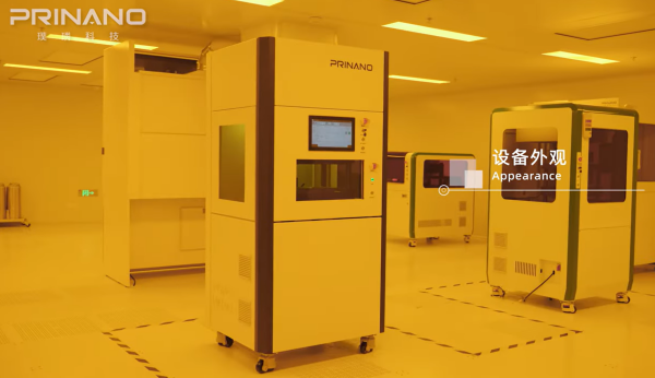
Prinano said the "PL-AS vacuum air-cushion nanoimprint lithography" equipment used this time can achieve resolution below 10 nanometers (nm). It also stressed it had succeeded in producing photonic chips for optical communications and LiDAR at the wafer level.
The company is also highlighting that the technology is being applied in industrial settings rather than remaining at the research stage, as it supplied NIL-based semiconductor manufacturing equipment to customers last year.
Some in the industry say the result should be assessed cautiously. Prinano highlighted cost savings but did not disclose key metrics such as actual production yield and throughput, and a mass-production schedule. In semiconductor manufacturing, stable mass-production capability determines competitiveness more than a technology demonstration.
Semiconductor analysis firm SemiAnalysis also assessed that NIL may be cost-competitive in certain areas but would not be easy to replace ASML's EUV equipment in cutting-edge semiconductor manufacturing. It said commercial competitiveness would be hard to secure without throughput, yield and process-integration capabilities.
NIL technology is not unique to China. Japan's Canon and Dai Nippon Printing, and memory chipmaker Kioxia are also jointly researching NIL-based semiconductor processes, and some production sites are conducting commercialization verification.
The industry is focusing on the possibility that NIL could be used as a complementary technology to cut costs and simplify processes in specific areas such as photonic chips and memory, rather than fully replacing advanced lithography equipment.
The announcement is seen as an example showing China's semiconductor industry is speeding up efforts to secure its own technology despite export controls on advanced equipment. Still, it appears that more concrete data disclosures on yield, production volume and mass-production timelines will be needed to judge its industrial significance.