Industry
Applied Materials expands packaging equipment lineup to boost HBM, chiplet yields
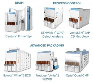
Applied Materials unveiled six new semiconductor manufacturing tools spanning advanced packaging and DRAM processes, the company said on Sunday. It said AI computing faces a “memory wall” as bandwidth and capacity lag growing model sizes and data throughput, driving demand for high-bandwidth memory and 3D stacking. The lineup includes CMP, electrochemical deposition and PECVD systems, two e-beam metrology tools, and an upgraded epitaxy system for DRAM peripheral transistors.