Search results for ALD
Industry
Applied Materials launches new tools to improve AI chip performance
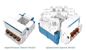
Applied Materials has introduced two new semiconductor process systems aimed at addressing uniformity challenges in high-stack 3D chip structures as demand for AI chips grows. The company unveiled the Centris Spectral SiN atomic layer deposition system and the Producer Selectra molybdenum etch system. It said the tools support transitions to vertical chip architectures such as GAA transistors and high-stack 3D NAND by improving deposition and etch uniformity in deep, narrow structures.
Industry
Applied Materials unveils two deposition systems for sub-2 nm GAA processes
Applied Materials on Monday unveiled two deposition systems tailored for sub-2 nanometre gate-all-around (GAA) transistor processes. The company said GAA transistor fabrication requires more than 500 process steps to build internal 3D structures, with many steps demanding near-atomic tolerances. One system uses selective bottom-up silicon nitride deposition to protect shallow trench isolation structures and reduce parasitic capacitance. The other controls metal gate stacks with atomic-level uniformity and integrates multiple metal deposition steps on one platform.
Industry
Chipmetrics targets South Korea as 3D NAND heads toward 1,000 layers
Finnish semiconductor metrology startup Chipmetrics is targeting South Korea as 3D NAND stacking moves beyond 300 layers toward 1,000. It aims to measure thin-film quality inside deep, narrow holes with a method it says is hundreds of times faster than conventional cross-section TEM analysis. CEO Mikko Utriainen said precise measurement will be key as aspect ratios rise. CTO Feng Gao said fabs often measure only planar uniformity, not conformality in 3D structures.