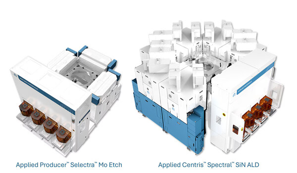
Amid intensifying competition in 3D semiconductor process equipment driven by growing demand for AI chips, Applied Materials has released new systems designed to address process-uniformity problems in high-stack structures. Applied Materials on Monday unveiled the Centris Spectral SiN atomic layer deposition (ALD) system and the Producer Selectra molybdenum etch system, it said.
Applied Materials said the spread of AI computing is accelerating a shift to vertical chip architectures such as gate-all-around (GAA) transistors and high-stack 3D NAND. As structures become deeper and narrower, conventional deposition and etch processes make it difficult to distribute materials uniformly from top to bottom. The variation leads to weaker electrical performance and lower yields.
The Centris Spectral SiN ALD system uses microwave plasma technology to address the issue. Existing plasma-enhanced deposition methods have struggled to avoid a trade-off in which higher plasma density in high aspect-ratio structures increases ion damage. The new system minimises that trade-off and deposits a dense silicon nitride (SiN) film uniformly at low temperatures even in narrow, deep structures. In GAA transistors, it is used to form a high-quality liner for transistor contacts to reduce resistance and capacitance and increase operating speed. The system was developed on Applied's Spectral ALD platform, and leading chipmakers are adopting it.
The Producer Selectra molybdenum etch system aims to shift the 3D NAND wordline separation process from wet to dry. As NAND stack counts rise, molybdenum, a low-resistance metal, is being used for wordline wiring, but conventional wet etching has caused a so-called 'top-heavy' profile because liquid chemicals fail to reach the entire deep structure evenly, concentrating etching at the top. The new system uses advanced gas delivery technology to secure uniformity across the top and bottom of the structure and reduce cell-to-cell variation to address leakage current and data retention issues. The company said it has already completed validation in a mass-production environment.
Prabu Raja (프라부 라자), president of Applied Materials' Semiconductor Products Group, said chipmakers are looking for new ways to deposit materials precisely and remove them selectively in extremely complex 3D architectures, from transistor structures to memory stacks. He said Applied provides differentiated capabilities through its latest deposition and selective etch systems to help customers overcome key scaling challenges and accelerate next-generation innovation in logic and memory.