
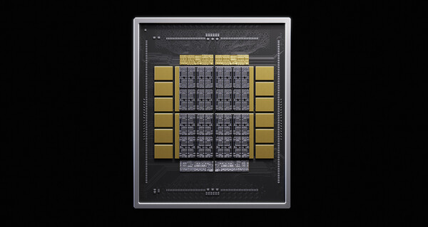
Nvidia is bringing the control circuitry of high-bandwidth memory (HBM) into its own design. Nvidia said on Aug. 26 local time on its blog that it will add next-generation HBM technology called NVHBM to NVLink Fusion, an interconnect technology between semiconductors.
HBM is memory that stacks DRAM vertically to increase data-processing speed. Nvidia said it will set a standard implementation of NVHBM, and major memory partners will validate it and supply it.
NVHBM changes where the memory controller is located. In the existing HBM structure, the controller that manages memory sits on top of the XPU die, the compute chip. XPU refers to a customised processor designed for a specific task. NVHBM integrates a custom controller designed by Nvidia into the HBM base die. The controller is placed inside the HBM stack structure built up in 3D.
Nvidia said the structure increases memory bandwidth by up to 30 percent versus HBM4E and reduces HBM power consumption by 15 percent. It also frees up up to 25 percent of area on the XPU compute die. That effectively reallocates silicon area previously taken by the controller to compute circuits. The three figures are all values presented by Nvidia, and third-party verification results were not disclosed.
Nvidia said it created a single standard implementation so multiple memory suppliers can release NVHBM to the same specification. Companies making custom chips can reduce work to integrate and validate memory separately for each supplier. Nvidia said the structure brings forward the launch timing for custom AI chips made by NVLink Fusion customers. It becomes a structure in which Nvidia specifications, rather than the chip designer, determine internal memory control methods.
NVLink Fusion is a technology that connects XPUs and CPUs made by external companies to Nvidia's rack-scale platform. Participants can use NVLink chiplets, NVLink-C2C, NVLink switches, and MGX systems and racks. An ecosystem spanning CPU partners, ASIC designers and system manufacturers is also provided.
NVHBM is developed on the same foundation as the technology Nvidia plans to apply to its own GPUs in the future. Nvidia said it plans to expand the application of this technology to NVLink Fusion customers. The company said that as AI agents and 1 trillion-parameter-scale workloads become common, compute performance alone does not determine AI infrastructure performance. It said computing, memory, storage, networking and software must be designed together as a single system.
Nvidia sets standard specification...Amazon's Annapurna Labs is first partner
Amazon semiconductor design unit Annapurna Labs is the first to join NVHBM cooperation. Within the scope of its cooperation with Nvidia around NVLink Fusion, Annapurna Labs will work on NVHBM technology and the NVLink scale-up structure. Nafea Bshara (나페아 브샤라), a vice president at Annapurna Labs, said, "NVHBM is a new architectural approach to raising the performance and efficiency of high-bandwidth memory," and added, "We expect this technology cooperation to help future AWS infrastructure design."
Annapurna Labs will support NVLink Fusion starting with its next-generation in-house chip, Trainium4. In the structure, chips designed by Amazon and Nvidia GPUs operate together within the same rack-unit structure. The cooperation is an extension of an earlier plan AWS disclosed to support NVLink Fusion. Nvidia said the structure allows participating companies to focus resources on XPU development while using a validated bundle of networking, rack systems and software.
 Daegeon Seok
d2dg@d-today.co.kr
Daegeon Seok
d2dg@d-today.co.kr