
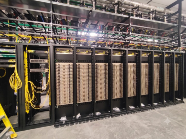
Nvidia is putting its own CPU directly into semiconductor design processes to speed development of next-generation chips. Nvidia said on July 27 it optimised key electronic design automation (EDA) applications with semiconductor design software companies Cadence and Synopsys.
As CPUs, GPUs and AI systems become more complex, the computing burden of designing the latest chips is also rising. Before a chip reaches the manufacturing stage, engineers validate and refine designs through thousands of iterations over several years. GPUs and AI have accelerated some areas, but core EDA workloads such as logic simulation and formal verification still depend heavily on CPU performance.
Nvidia is introducing its Vera CPU across EDA workflows used to develop next-generation CPUs and GPUs. The tests included Cadence's formal verification platform Jasper and Synopsys' functional verification solution VCS, and both applications recorded up to 1.5 times higher performance on some workloads based on the same number of cores.
The Vera CPU combines 88 custom Olympus CPU cores with an LPDDR5X memory subsystem and a second-generation scalable coherent fabric. It is designed to deliver high per-core performance and memory bandwidth for workloads that mix latency-sensitive tasks and large-scale regression tests. Faster execution can allow engineers to review more design alternatives and complete verification work within the same development period.
Nvidia said it is continuing application profiling, software optimisation and system-level tuning with Cadence and Synopsys. It plans to advance Vera through a next-generation Rosa CPU while continuing to optimise major EDA applications across its CPU roadmap.
 Dae-geon Seok
d2dg@d-today.co.kr
Dae-geon Seok
d2dg@d-today.co.kr