
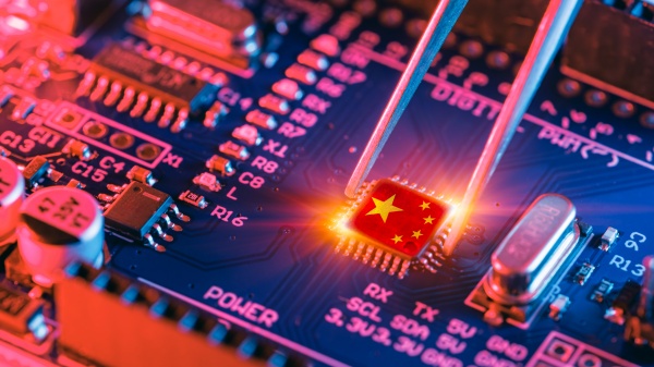
[DigitalToday reporter Jinju Hong (홍진주)] Chinese semiconductor startup Yuanjiyue unveiled what it billed as the world’s first 8-inch pilot production line for 2D semiconductors. It also set a goal of developing chips with 5-nanometre-class performance by 2029 without extreme ultraviolet (EUV) lithography equipment.
The Hong Kong-based South China Morning Post reported on July 11 that Shanghai-headquartered Yuanjiyue announced plans on July 10 on its WeChat account to build an 8-inch pilot production line for 2D semiconductors.
The company said the line was designed to support the entire process, from preparing 2D materials to chip integration and tape-out. It claimed it would be the world’s first 8-inch production line for 2D semiconductors. The announcement is interpreted as a push to industrialise next-generation semiconductor technology that differs from existing silicon processes, as U.S. export restrictions on advanced semiconductor equipment have made it difficult for China to secure EUV lithography tools.
Yuanjiyue said building the line means 2D semiconductor technology has moved beyond laboratory research into engineering verification and industrial production. The company described it as an important milestone for China’s self-reliance in core semiconductor technologies.
As advanced chipmaking faces physical limits and rising manufacturing costs, the semiconductor industry is seeking new structures to replace or complement existing silicon-based semiconductors. 2D semiconductors are also drawing attention as one of these next-generation technologies.
Yuanjiyue also outlined a commercialisation timeline. Chairman Bao Wenzhong (바오원중) said it aims to establish a manufacturing process this year equivalent to a 90-nanometre silicon process. He said it aims by 2029 to develop a fully domestic process that can deliver 5-nanometre-class performance without EUV equipment.
2D semiconductors use materials with atomic-scale thickness. They are seen as making it easier to implement smaller transistors than in existing silicon-based semiconductors and to improve power efficiency. Bao said the thinness of 2D materials makes it possible to miniaturise devices without applying complex transistor structures. He added that ultra-low leakage characteristics can sharply reduce power consumption, and that combining the technology with 3D stacking could also help improve memory density.
Leakage current is a major problem that worsens as silicon semiconductors are scaled down. Current flows even when transistors are off, increasing power consumption and heat generation. Yuanjiyue expects 2D semiconductors could be an alternative that overcomes these limits.
The Chinese government is also attaching significance to the technology development. Pan Hao (판하오), who oversees advanced materials at the Shanghai Municipal Science and Technology Commission, said at the production-line unveiling event, "2D semiconductors are assessed as one of the most promising technologies for next-generation semiconductors, and global competition is growing increasingly fierce."
Still, there are many challenges to overcome before commercialisation. Industry participants believe that without building a supply chain covering materials and equipment, design, manufacturing and testing, it is difficult for a single company to commercialise the technology.
Because the semiconductor industry requires process verification and ecosystem building to proceed together, a key point to watch will be whether Yuanjiyue’s 2029 roadmap can translate into actual mass-production competitiveness.
 Jinju Hong
hongjj@d-today.co.kr
Jinju Hong
hongjj@d-today.co.kr