
A South Korean research team has developed a structure that could ease an “electrical bottleneck” that reduces performance and power efficiency in next-generation semiconductors.
KAIST said on July 13 that a team led by Professor Seungbeom Hong (홍승범) of the Department of Materials Science and Engineering, working with teams led by Professor Kibum Kang (강기범) and Professor Seongbeom Cho (조성범) of Sungkyunkwan University, built a structure in 2D materials that allows electricity to flow without obstruction and developed an analysis platform that can directly observe it.
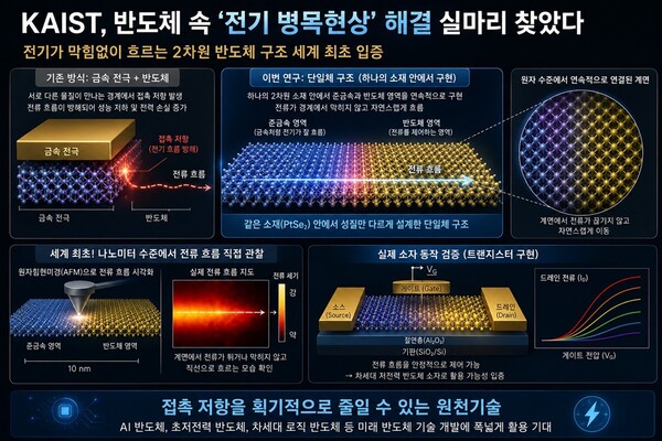
Semiconductors suffer performance declines and power loss due to contact resistance at the boundary where a metal electrode meets the semiconductor. As semiconductor devices shrink, the impact of contact resistance grows, making it a key challenge in developing next-generation semiconductors.
The team implemented semimetal and semiconductor regions continuously within a single thin film of platinum diselenide (PtSe2), a 2D material with atomic-layer thickness. By creating a unified structure in which the two regions connect naturally within the same material, it presented a new structure that allows current to flow without being blocked at the boundary.
Using an atomic force microscope (AFM), the team visualized charge movement within the thin film at the nanometre level. It confirmed that when current moved from the semimetal region to the semiconductor region, the flow continued naturally without a bottleneck in which it was blocked or bent in direction.
The team also verified operation by applying an electric field to the semiconductor region like a transistor. Experiments showed that current flow could be controlled stably in a structure combining semimetal and semiconductor regions.
The team expected the technology to be used to develop AI semiconductors, ultra-low-power semiconductors and next-generation logic semiconductors by reducing contact resistance in 2D-material-based semiconductor devices.
Seungbeom Hong of KAIST said it was the world’s first case of directly confirming, at the nanometre level, how current flows at a 2D semiconductor interface. He said it is expected to be used as a core foundational technology to solve contact resistance problems in various next-generation semiconductors.
The research involved KAIST doctoral student Yeon-gyu Kim (김연규), Minseung Kyeon (견민승) and Sungkyunkwan University doctoral student Jihoon Hong (홍지훈) as co-first authors. The results were published in the July 2026 issue of the international materials science journal Matter.
 Jin-ho Lee
jhlee26@d-today.co.kr
Jin-ho Lee
jhlee26@d-today.co.kr