
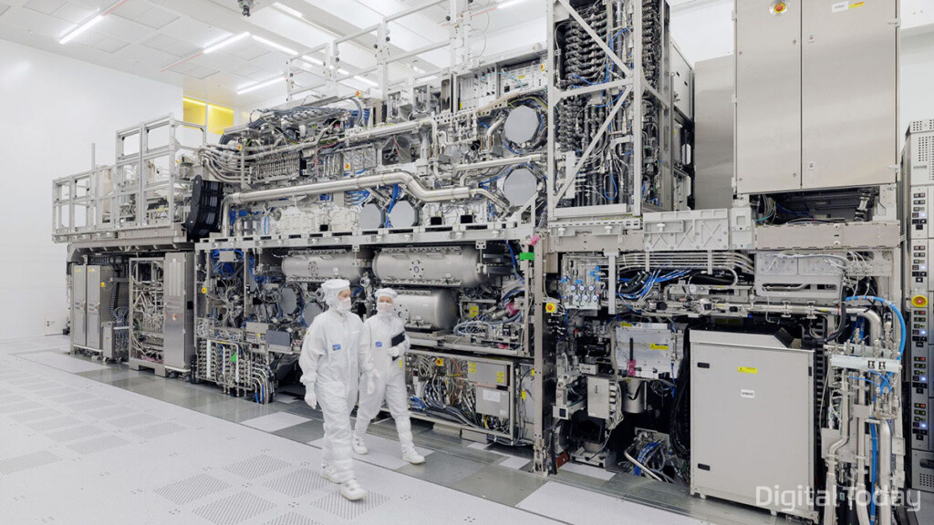
Technology and production preparations in the mask industry tailored to ASML's next-generation High-NA EUV lithography tools are accelerating. As DRAM makers and foundries increasingly firm up timelines for adopting the equipment, mask manufacturers are also disclosing their technology and production capabilities for the new tools. Japanese companies have effectively monopolised the EUV mask materials market, but Korean companies are now preparing to enter by obtaining certifications for existing EUV pellicles and blank masks.
Industry plans for introducing High-NA EUV into mass production are being set in stages from 2028, according to the industry on Oct. 26. Dutch semiconductor publication Bits&Chips reported that DRAM makers, including Samsung Electronics, will begin full-scale High-NA EUV ramp-ups from 2028. Ramp-up is the stage of bringing in equipment and raising output.
High-NA EUV tools are lithography systems that boost the ability of lenses to gather light, enabling finer circuits to be printed on wafers. Fine patterns that are difficult to draw in a single pass with existing tools are split across multiple exposures, but High-NA EUV can reduce this to a single exposure.
For memory makers, High-NA EUV is used to draw cells more densely to raise integration while reducing process steps. The current mainstay for mass production in leading-edge logic and DRAM processes is existing EUV equipment. Global DRAM makers have already outlined High-NA EUV adoption schedules. Samsung Electronics' P5 and SK Hynix's Y1, among new domestic DRAM fabs, will also begin equipment investment in earnest from next year, according to SK Securities.
Logic makers are also finalising adoption schedules. Intel will shoulder the cost and risk of early adoption to regain technology leadership and start mass production 2 years ahead of TSMC. TSMC, which has repeatedly criticised the high price of the equipment publicly, has decided to begin mass production in 2030. According to SK Securities, Nvidia's next-generation graphics processing unit Rubin has a die of about 858 square millimetres, reaching lithography limits. Logic companies that handle large chips have effectively decided to adopt the tools despite the burden of having to split chips in half for printing and then stitch them together. Samsung Electronics' foundry business is also setting a schedule similar to TSMC's.
As equipment adoption schedules for global memory companies are set one after another, the key preparations are shifting to masks. A SEMI photomask report cited building up technology and production readiness in line with High-NA EUV adoption schedules as a key task for mask manufacturers.
Demand for EUV masks is already increasing. SEMI analysed that mask production facilities operated directly by chipmakers are increasing EUV mask production capacity to meet demand for leading-edge logic and memory. According to SEMI, the share of EUV masks by volume in the photomask market rose from about 1 percent in 2020 to about 7 percent in 2025.
Japanese companies have monopolised the materials used in these masks. According to SK Securities, EUV-related materials are currently supplied in a structure effectively dominated by Japanese companies. In the blank mask market, which provides photomask raw materials, Japanese companies Shin-Etsu MicroSi, Hoya and AGC account for about 86 percent by 2025 revenue, according to QY Research.
Blank masks require long-term quality certification by customers on substrate flatness and micro-defect control technology, making it difficult for new companies to enter. For EUV, dozens of multilayer reflective films must be stacked, making them harder to produce than DUV products. Hoya has already built mass-production experience, with EUV products accounting for 29 percent of blank mask revenue in the first quarter of fiscal 2019.
Korean materials companies are also preparing to enter the EUV mask materials market. According to SK Securities, FST is expected to enter the market next year after obtaining ASML certification within this year for its carbon nanotube-based EUV pellicle, a mask protective film. The company has secured pellicles with the transmittance and high-power performance required by the market. In the first quarter of next year, FST's EUV-related infrastructure equipment is scheduled to be installed on leading-edge foundry lines at major customers. SK Securities estimated that the CNT-based EUV pellicle market, based on major customers, will grow from 35 billion won in 2027 to more than 90 billion won in 2028.
S&S Tech is expanding its business scope from blank masks to EUV. The company completed an EUV-dedicated centre in Yongin in October last year and aims to finish customer qualification tests for its EUV blank masks early next year. The Korea IR Council forecast that production capacity will roughly double from the current level once the Yongin centre comes online. Its EUV pellicle also entered customer quality tests in September. However, blank mask certification was expected to be applied in the second quarter of this year but was delayed once. As supply track records in existing EUV are needed to enter the High-NA mask ecosystem, this certification timeline is a variable for gauging the pace of preparation by Korean companies.
 Daegeon Seok
d2dg@d-today.co.kr