
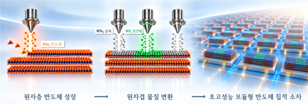
A technology has been developed to selectively replace atoms that make up semiconductors and implement multiple electrical functions on a single thin film.
The Ministry of Science and ICT said on Thursday that a research team led by Jo Moon-ho (조문호), head of the Van der Waals Quantum Matter Research Group at the Institute for Basic Science (IBS), developed a "modular transistor fabrication technology" that selectively substitutes atoms in 2D semiconductors. The findings were published the same day in the international journal Science.
2D semiconductors can control current even at atomic-layer thickness, drawing attention as a next-generation material that could overcome the miniaturisation limits of existing silicon semiconductors. Making practical devices has been difficult because it requires precise integration of different materials such as semiconductors, insulating films and metal electrodes.
Instead of stacking different materials, the team devised a method to directly create the needed materials by replacing atoms in an existing semiconductor. It succeeded in substituting selenium atoms in tungsten diselenide (WSe2) with oxygen, sulfur and tellurium, among others, to form an insulator, a semiconductor and a semimetal at desired locations. In particular, it transformed materials in atomic layers about 0.7 nanometres thick by controlling reaction temperature and gas pressure. Using masks for semiconductor processing also makes it possible to selectively change only specific locations.
Using the approach, the team built a transistor on a single thin film that includes a semiconductor, an insulating film and an electrode junction layer. The voltage swing required to switch current on and off was 61.3 millivolts, close to the theoretical room-temperature limit of about 60 millivolts. The ratio between the on state and the off state exceeded 10 million.
It reduced the energy barrier between the electrode and the semiconductor to about one third of the level in conventional methods that directly bond metal electrodes. It also achieved an equivalent oxide thickness (EOT) of less than 1 nanometre in the insulating film, securing performance needed for ultrafine semiconductors. The team also built a complementary inverter by stacking p-type and n-type transistors vertically. The device operated at a low voltage of 1 volt, confirming the potential for expansion into 3D stacked integrated circuits.
The team plans to apply the technology to various 2D semiconductor materials and develop it into a wafer-scale, large-area process.
Jo, an IBS group leader, said the study was meaningful in that it applied basic materials science techniques of atomic-scale manipulation to modern semiconductor technology. He said it could be extended to next-generation stacked semiconductor device technologies as well as ultra-low-power and ultrafine semiconductors.
 Jin-ho Lee
jhlee26@d-today.co.kr
Jin-ho Lee
jhlee26@d-today.co.kr