
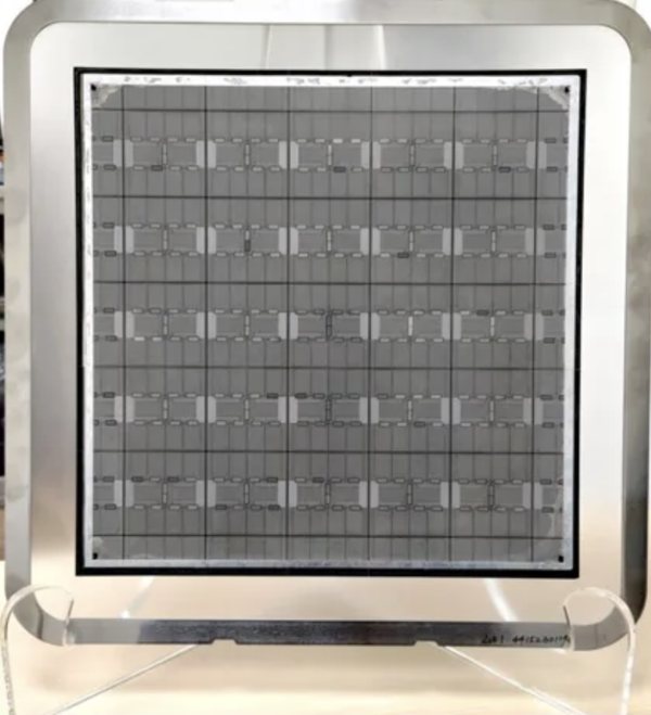
[DigitalToday reporter Dae-geon Seok (석대건)] As AI chips grow in area, line investment is starting at home and abroad to switch packaging bases from round wafers to large-area square substrates. Using square panels can process 5 to 6 times more chips at once than existing wafers, and area utilisation rises to 87 percent from 57 percent. Competition between Taiwanese and South Korean companies over panel-level packaging, which enables this process, is also intensifying.
The shift in technology flow to square panels is driven by area. Chips are cut into rectangles, but wafers are round, so a 300 mm (12-inch) round wafer cannot avoid space being cut off at the edges. Panel-level packaging is a process that breaks free of this constraint. Unlike the existing method of applying wiring on a wafer before cutting chips, it rearranges already cut chips on another plate and adds moulding and redistribution layers (RDL).
Because it is made square from the outset using organic or glass substrates, there is no leftover space after filling with chips. For example, using a 600 by 600 mm square panel can process 5 to 6 times more chips at once than a wafer, and area utilisation rises to 87 percent from 57 percent.
Counterpoint Research forecasts that the market combining fan-out panel-level packaging (FOPLP) and glass substrates will grow from $650 million in 2024 to more than $8.1 billion in 2030. Of that, AI and high-performance computing (HPC) account for 45.6 percent, and 84.8 percent of panel-level production capacity in 2030 is tallied as concentrated in Taiwan, Japan and China.
TSMC has started operating this year a CoPoS pilot line expanded to square panels. It brought in the first equipment in February at its affiliate VisEra’s Yongdam plant, completed the line in June and began small trial production in the first half, then moves it to the Zhainan AP7 plant to verify the process.
TSMC Chairman C.C. Wei (위자충) said on an April earnings conference call that mass production of panel-level fan-out takes 2 to 3 years. According to DigiTimes, the mass-production timing is late 2028 to early 2029 and the first customer is Nvidia. The goal is to package 12 units of fourth-generation high-bandwidth memory (HBM) and GPU chiplets together in the Feynman architecture expected around 2028.
According to the industry, Samsung Electronics is also shifting the development axis of 2.5D packaging from wafer-level packaging (WLP) to panel-level packaging (PLP). Samsung Electronics took over the panel-level packaging business from Samsung Electro-Mechanics and has first applied it to mobile application processors and power management integrated circuits (PMIC). According to Semiconductor Engineering, FOPLP was used in the Exynos W920 for wearables along with a 5-nanometre extreme ultraviolet (EUV) process.
Investment in panel lines has opened a new equipment market. According to Semiconductor Engineering, building a single FOPLP line costs more than $100 million to $200 million, and the equipment is not compatible with existing 300 mm processes, making it difficult to recoup investment if utilisation is low. Panel sizes also vary from 400 by 500 mm to 650 by 650 mm, creating room for additional equipment builds as tools must be reconfigured for each specification.
According to DigiTimes, about 30 companies in Japan, the United States, Germany and Taiwan are candidates for TSMC’s first CoPoS equipment evaluation, spanning all six major process areas including lithography, copper plating, polishing and inspection. South Korean equipment makers also see this phase as an order opportunity. Hanwha Semitech moved in earnest to enter the market by unveiling for the first time the actual 600 by 600 mm large-area FOPLP tool, the 'SFM5 Square', at SEMICON Taiwan 2026 held in Taipei, Taiwan on Sept. 2 to 4. An industry official said, "The 2 to 3 years in which the Taiwan camp refines processes on a pilot line is the period when South Korean equipment makers must prove their ability to respond to each specification."
 Dae-geon Seok
d2dg@d-today.co.kr
Dae-geon Seok
d2dg@d-today.co.kr