
Chinese power semiconductor companies that have expanded the market with low-priced supply are turning to price increases, a shift expected to add momentum to domestic companies' conversion to 8-inch (200 mm) silicon carbide (SiC). The government has also begun upgrading public fab infrastructure, centred on the southern region.
Chinese power semiconductor companies recently notified customers of price increases of about 10 to 25 percent, the industry said on Aug. 13. Global top players such as Texas Instruments and Infineon have also announced plans to raise prices by 10 to 20 percent. Kiwoom Securities analysed that it means Chinese companies that expanded share with low-priced supply have begun exercising pricing power.
The driver behind the increases is demand from artificial intelligence (AI) data centres. Kiwoom Securities analysed that among AI server components, supply shortages have spread from graphics processing units (GPUs) to memory, central processing units (CPUs) and FC-BGA substrates, and then to multilayer ceramic capacitors (MLCCs) and power semiconductors. It also pointed to Nvidia's push to shift to an 800VDC architecture as a factor increasing the use of power semiconductors.
Demand from data centres is also strong. As power consumption rises per chip and per architecture, instability in frequency and load-variation control has come to the fore. DC blocks and solid-state transformers (SST) using wide-bandgap power devices are being discussed as responses, drawing attention to power semiconductors.
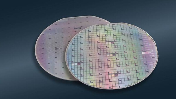
In a period of rising prices, shifting to 8-inch wafers is a way to change the cost structure. An 8-inch wafer produces about 1.9 times as many chips as an existing 6-inch wafer and can cut costs by more than 30 percent, the industry said. China has already built a mass-production system for 8-inch wafers and is pursuing development of 12-inch technology in parallel.
In South Korea, production schedules are also taking shape. Samsung Electronics is expected to begin full operation of an 8-inch gallium nitride (GaN) contract manufacturing line from the second quarter of this year, and sample mass production of planar-structure SiC MOSFETs is being discussed for the third quarter. DB HiTek is expected to start mass production of GaN foundry output in the second half of this year, and SK Key Foundry has secured device characteristics for 650V GaN high-electron-mobility transistors (HEMT).
The global landscape is also shifting. TSMC has decided to gradually halt its GaN contract manufacturing business by July 2027 to focus its capabilities on 300 mm leading-edge processes and advanced packaging in response to AI demand. Related technology has been transferred to its affiliate VIS.
Market size forecasts are also being revised upward. Fortune Business Insights projected the SiC power semiconductor market would grow at a compound annual rate of 17.7 percent from $4.02 billion in 2025 to $18.61 billion in 2034. TrendForce forecast GaN power semiconductors would rise at a compound annual rate of 49 percent from $270 million in 2023 to $4.38 billion in 2030.
From ingot slicing to 1,700 degrees Celsius heat treatment ... yield drives costs
But the shift to 8-inch is not just a matter of increasing wafer size. SiC is stronger than silicon, making it difficult to slice ingots thinly and polish surfaces in the chemical mechanical planarisation (CMP) process. Epitaxial growth, which builds a high-purity crystal layer on the wafer, is a process found only in power semiconductors, and thicker epitaxial layers increase voltage endurance. Ion implantation is also difficult at room temperature, requiring activation through heat treatment at temperatures above 1,700 degrees Celsius. Many chips use a vertical structure in which the back side acts as an electrode, so a process to thin the wafer back side follows. Even if larger diameters theoretically reduce costs, the savings are offset if defect rates are not controlled in these steps.
Still, there is criticism that South Korea has not established a leading demand company to drive SiC power semiconductors. The absence of integrated device manufacturers (IDMs) like Infineon and STMicroelectronics that cover design through manufacturing, and a foundry-centred structure, mean line utilisation rises only when customer volumes are secured. This is the background to the Industry Ministry planning integrated, end-to-end R&D in this roadmap linked to demand companies in areas such as electric vehicles, defence, power grids and data centres.
The government has also moved to support infrastructure. The Ministry of Trade, Industry and Energy held a next-generation power semiconductor forum in April and disclosed progress on its roadmap to foster the next-generation power semiconductor industry. The ministry said the roadmap includes a plan for large, integrated R&D spanning materials, devices, modules and system demonstration, as well as measures to build infrastructure centred on regional hubs.
The hub is the southern region. The ministry plans to upgrade public fab infrastructure in the Busan power semiconductor specialised complex and support the use of demonstration data secured at existing public infrastructure in places such as Pohang and Naju in private-sector mass production. According to Yuanta Securities, the government will invest 260.1 billion won in compound semiconductor development from 2025 to 2031.
Woo-hyuk Choi (최우혁), director general for advanced industrial policy at the ministry, said, "As the reorganisation of the global supply chain surrounding power semiconductors accelerates, we will push compound semiconductors as a key development task while building an ecosystem to foster the power semiconductor industry together with relevant ministries, centred on the southern power semiconductor innovation belt."
At the government level, it also decided to place next-generation power semiconductors as a key task of the ultra-innovation economy project and move ahead with planning large-scale R&D. Yun-cheol Koo (구윤철), deputy prime minister and minister of finance and economy, said he chaired an emergency economic headquarters meeting and a meeting of economy-related ministers in June and discussed the "status and future plans for the ultra-innovation economy project". At the meeting, power semiconductors were handled as targets for demonstration support along with small modular reactors (SMRs), on-sensor AI, actuators for humanoid robots and secondary batteries, and the government has a policy of ensuring project results emerge starting next year.
 Dae-geon Seok
d2dg@d-today.co.kr
Dae-geon Seok
d2dg@d-today.co.kr