
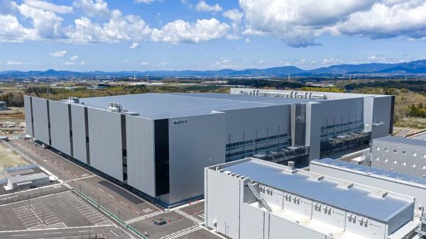
Sony Group and Taiwan's TSMC will set up a $4.69 billion joint venture in Kumamoto prefecture in Japan for next-generation smartphone image sensors. The strategy is to combine Sony's image-sensor technology with TSMC's advanced chipmaking capabilities to target the image-sensor market for smartphones as well as AI and automotive uses.
Cryptopolitan reported on Aug. 11 that Sony and TSMC signed a binding final agreement that day to establish a joint venture called Advanced Vision Semiconductor Manufacturing in Koshi, Kumamoto prefecture.
The joint venture will be run under a structure in which Sony holds management control. Sony Semiconductor Solutions, Sony's chip unit, will hold a controlling stake and bring the venture in as a Sony Group subsidiary. Sony will also take the lead in the board's composition.
Total investment will be 747 billion yen. Sony Semiconductor Solutions will invest about 465 billion yen, including a cash contribution and the transfer of assets through a corporate split, while TSMC will contribute about 282 billion yen.
TSMC's investment will not be deployed all at once. TSMC plans to disburse funds in stages, taking into account market demand and business conditions. It left room to adjust the pace of investment if orders in the image-sensor market or the business environment deteriorate more than expected.
Whether the Japanese government provides support is also a key condition for 추진 of the project. TSMC said setting up the joint venture is premised on sufficient support from the Japanese government. Sony and TSMC plan to request related support from Japan's Ministry of Economy, Trade and Industry.
The Japanese government has been continuing large-scale subsidies and policy support to expand the domestic chip production base. This joint venture is also seen as a project being pursued in tandem with the government's policy to foster the semiconductor industry.
The two companies' roles are also clearly divided. Sony Semiconductor Solutions will be responsible for core image-sensor technology and product planning and design. TSMC will handle mass production based on advanced semiconductor process technology and experience in large-scale manufacturing. The two companies plan to combine their strengths to speed up development and commercialization of image-sensor products tailored to customer demand. They also plan to expand applications beyond smartphones to AI, automotive and mobile fields.
The target for mass production is 2029. The joint venture will operate by adding new development and production capabilities based on Sony's existing image-sensor production facilities already built in Koshi, Kumamoto prefecture. The joint venture will also be closely linked to TSMC's semiconductor production base being formed in Kumamoto.
A first Kumamoto plant operated by TSMC's Japanese unit JASM began commercial operations in late 2024. The plant produces semiconductors using specialized processes, and a second plant is now under construction. The second plant targets mass production on a 3-nanometer process in 2028.
With Sony and TSMC building a joint image-sensor production base in the same area, the ecosystem linking semiconductor design and development with production around Kumamoto is expected to be further strengthened.
Kumamoto is already emerging as a key region in Japan's semiconductor supply chain. By combining Sony's image-sensor technology and production base near TSMC's production facilities, the two companies expect to improve efficiency from development through mass production and strengthen responsiveness to customers.
The two companies previously disclosed their cooperation plan through a non-binding memorandum of understanding in May. With this final agreement, they have turned that cooperation concept into a legally binding project.
This joint venture is assessed as a case in which three strategies intersect: fostering Japan's semiconductor industry, strengthening Sony's image-sensor competitiveness, and expanding TSMC's production base in Japan.
The pace of actual investment execution and the scale of production capacity expansion could vary depending on market conditions. As TSMC has said it will invest in stages depending on market demand and business conditions, image-sensor demand and the scale of Japanese government support are cited as key variables that will determine the pace of the project going forward.
 Jinju Hong
hongjj@d-today.co.kr
Jinju Hong
hongjj@d-today.co.kr