
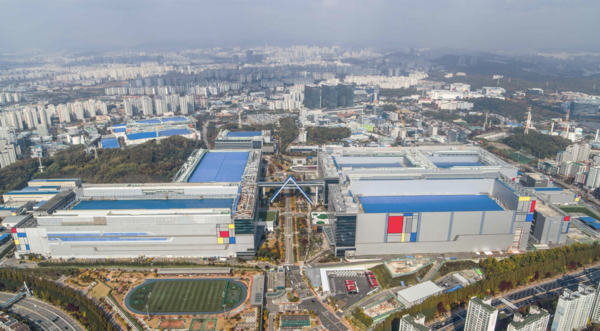
Samsung Electronics is seeking a turnaround in its foundry business with an "AI factory" turnkey model that bundles memory, foundry and packaging. With TSMC's 3-nanometre utilisation nearing 100% and price increases for advanced-process wafers expected, demand from fabless firms looking to cut reliance on a single vendor is emerging as an opportunity for Samsung Electronics. Whether it can begin mass production at 2 nanometres in the second half and make turnkey order wins visible is expected to be a turning point for its foundry business.
Industry sources said on Sunday that a new breakthrough is opening for Samsung Electronics' foundry business as orders pile up at TSMC. Demand for AI semiconductors is surging, but capacity for TSMC's advanced processes has hit its limits. As prices rise as well, fabless firms have begun looking for alternatives. For Samsung Electronics' foundry business, which has struggled with yields and customer acquisition, the shift in market dynamics is an opportunity. That is the backdrop for Samsung Electronics pushing into the gap with a turnkey strategy built around its memory strengths.
Samsung Electronics said on a first-quarter earnings conference call on May 30 that customer demand to secure memory and foundry as a turnkey offering is increasing. It added that it is discussing 2-nanometre and 4-nanometre processes with multiple high-performance computing (HPC) customers and that 2-nanometre contracts with some customers will become visible in the near term, it said.
The demand stems from a foundry market structure centred on TSMC. According to TrendForce, TSMC's 3-nanometre (N3) process utilisation is nearing 100%, leaving capacity saturated for the next 1 to 2 years on orders from Apple and Nvidia, among others. TrendForce forecast that TSMC will raise wafer prices for its advanced 3-nanometre and 5-nanometre processes by at least 5 percent, pointing to worsening profitability for fabless firms and pressure to raise chip prices.
As both pricing and supply-chain risks rise, moves to find alternatives are accelerating. Counterpoint Research analysed that as AI semiconductor demand explodes, the trend is strengthening for chip design companies to spread the risk of relying on TSMC as a single vendor. It also assessed that Samsung Electronics, which is preparing a 2-nanometre gate-all-around (GAA) process roadmap, is being cited as a leading "second source" candidate.
Samsung Electronics' key differentiator is the AI factory model it announced last year. The approach provides not only foundry contract manufacturing but also advanced memory (HBM) integration and advanced packaging (AVP) in a one-stop ecosystem. The company envisions reducing the time and logistics costs from chip design to final packaging, which could offer an alternative for fabless firms burdened by TSMC price increases.
The model's economics are being highlighted as the industry moves into the HBM4 era. According to the financial investment industry, the HBM4 era makes the combination of memory and foundry, or logic die integration, essential. As an integrated device manufacturer (IDM) that can perform foundry, HBM and packaging in-house, Samsung Electronics' one-stop turnkey solution is assessed to be able to cut customers' chip development time by about 20 percent and lower supply-chain management costs.
Samsung signals 2-nanometre contracts may take shape, but disclosing customers and volumes remains a task
Samsung Electronics forecasts that from the third quarter this year, HBM4 sales will exceed half of its total HBM sales. After succeeding in mass-production shipments of HBM4 in February, it has also begun supplying samples of next-generation HBM4E 12-high stacks to global customers. The HBM4E 12-high stack supports 48 gigabytes (GB) of capacity and 16 Gbps operating speed per pin, and applies the same 1c DRAM and 4-nanometre base die combination as HBM4 in mass production. The in-house structure from memory through logic die itself is the foundation of the turnkey model.
Production bases are also being built out in stages. Taylor Fab 1 held an equipment move-in ceremony on May 23, targeting operations in 2026 and mass production in 2027. Samsung Electronics plans to expand 2-nanometre capacity in phases after operations begin. By contrast, it is moving to streamline less competitive processes. Samsung Electronics is shifting capacity for CIS and display driver ICs (DDI) to 17 nanometres, and is sequentially closing lines for power management ICs (PMIC) and DDI, among others, that are in mass production on 8-inch wafers.
Still, it needs to be verified whether these efforts will translate into actual orders. Samsung Electronics has signalled that 2-nanometre contracts will become visible, but it did not disclose specific customers or volumes. An industry official said, "If the AI factory model succeeds, it is a practical alternative to TSMC's dominance, but if orders are delayed, the model could remain merely a declaration."
 Dae-geon Seok
d2dg@d-today.co.kr
Dae-geon Seok
d2dg@d-today.co.kr