
Samsung Electronics and SK hynix have presented different solutions for the next step after high-bandwidth memory (HBM).
The chip industry says Samsung Electronics and SK hynix have concluded that it is difficult to expand bandwidth and capacity at the same time with existing HBM alone as AI computing demand rises, and they are preparing responses. Samsung is focusing on easing data-movement bottlenecks through 3D vertical stacking that reduces the distance between memory and AI accelerators. SK hynix has opted for a strategy that raises overall system capacity and efficiency by placing and connecting different types of memory, such as HBM and high-bandwidth flash (HBF), in tiers.
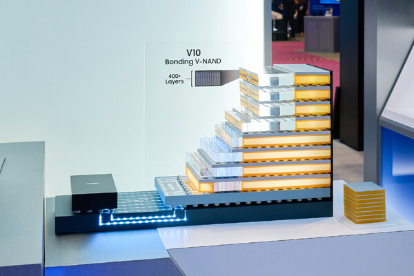
Samsung's zHBM moves away from placing HBM next to an AI accelerator (xPU) and instead stacks HBM vertically on top of the accelerator. HBM is memory that boosts data-processing speed by stacking multiple layers of DRAM. Samsung said an interface system using zHBM offers up to 8 times the performance and up to 3 times the performance per watt of eighth-generation HBM5, with thermal resistance less than half. Samsung also unveiled 'zNAND-O', which combines through-silicon vias (TSV) with V-NAND, and the 10th-generation 'V10 BV-NAND' with more than 400 layers.
SK hynix and SanDisk released the first standard specification for HBF. Unlike HBM, which stacks DRAM, HBF is made by vertically stacking NAND flash, creating a new tier between fast HBM and high-capacity SSDs. The standard defines maximum capacity of up to 512GB based on two configurations that stack NAND dies in 8 layers and 16 layers. It also supports bandwidth of 0.4 to 3.0 terabytes per second across three grades. It adopted UCIe, an open standard, as the method to connect to processors. The specification was released through the Open Compute Project (OCP), and the consortium includes Google and Tenstorrent.
WHY: A physical limit drives shift away from proven HBM
The companies are changing the structure itself because they believe the existing approach has reached physical limits. Kim Kyung-ryun (김경륜), a managing director in Samsung Electronics' DRAM development team, introduced the 3D architecture zHBM in a keynote at 'FMS 2026'. "Customers are demanding memory performance that is 10 times higher, but there are limits to existing 2.5D structures such as HBM4 and HBM5," he said. "The only breakthrough to overcome this is a 3D vertical stacking structure." He said when accelerators and memory sit on the same plane, the distance data must travel is longer, increasing time and power use.
The limitation was reaffirmed at the semiconductor design conference 'Hot Chips 2026 (Hotchios 2026)' being held in the United States. At Hot Chips 2026, power consumption and scalability limits of HBM were a major topic. While HBM is widely used in high-performance computing, participants shared the view that structural innovation is needed because existing designs are reaching limits in power efficiency and capacity expansion.
Samsung also provided specific figures on improvements in power efficiency for zHBM in a Hot Chips 2026 presentation. Assuming a configuration in which 4 HBM stacks are placed on 1 GPU, zHBM can cut DRAM power by 100 watts compared with existing HBM4E, it said. Samsung said the I/O power savings result from eliminating the serializer-deserializer (SERDES) structure between the accelerator and memory, and that the saved power can be used to secure headroom for computing performance and heat generation.
A lack of supply is also pushing the shift. Kiwoom Securities forecast that the HBM demand growth rate in 2027 will be 56 percent, exceeding the 50 percent supply growth rate, widening shortages, and that the average market price of HBM4 will rise 65 percent. That means the approach of improving performance by adding more HBM has hit a wall in both supply volume and cost. Adjustments have already begun. Eugene Investment & Securities analysed Nvidia's decision to lower the amount of HBM in its next-generation Rubin Ultra accelerator as the result of HBM supply failing to keep up with the accelerator production plan.
SK hynix also cited this in putting HBF forward. If temporary data referenced when AI generates an answer is moved down to the NAND tier instead of using expensive HBM, more data can be handled at the same cost. Eugene Investment & Securities said such data migration will spread as DRAM and HBM shortages worsen, raising NAND demand as well.
The different approaches leave the two companies with different problems to solve. Samsung faces the burden of controlling heat because it places memory on top of heat-generating accelerators. Samsung applied a design that reduces the number of DRAM stacking layers compared with existing HBM to reflect that.
SK hynix needs to increase the number of companies that will use the standard. SanDisk, a development partner, has completed the design of the first HBF memory die and will supply initial samples for AI inference to customers in 2027. It also laid out plans to begin mass production of enterprise SSDs using the technology in early 2027.
There is also a forecast that DRAM itself will be developed as a product tailored to specific companies. Eugene Investment & Securities analysed that the trend toward 3D-stacked DRAM will shift development from a general-purpose product to a custom product developed from the outset together with specific semiconductors. It forecast that suppliers capable of supporting specific semiconductors will be narrowed, as memory makers must take part from the early stages of development and the cost of switching a chosen supplier rises.
 Daegeon Seok
d2dg@d-today.co.kr
Daegeon Seok
d2dg@d-today.co.kr