
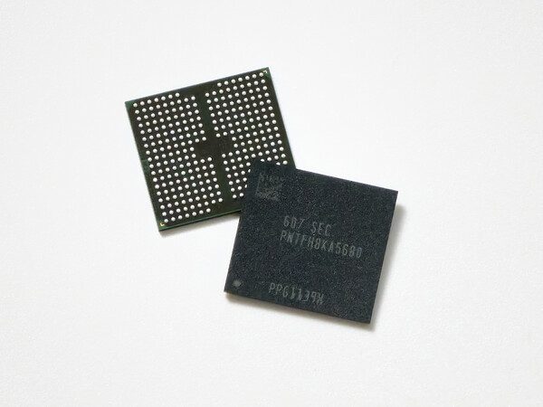
[DigitalToday reporter Daegeon Seok] Samsung Electronics has unveiled next-generation 3D memory technology to respond to the spread of AI infrastructure. Samsung Electronics said on Aug. 4 it was taking part in FMS (Future of Memory and Storage) 2026, held from Aug. 4 to 6 (local time) at the Santa Clara Convention Center in Santa Clara, California, and for the first time in the industry revealed mock-ups of its next-generation 3D memory architectures, zHBM and zNAND-O.
Samsung Electronics set up a booth shaped like an AI cloud server in an exhibition space of about 66 square meters and showcased about 30 products. At 11:40 a.m. on Aug. 4 (local time), the first day of the event, Vice President Jin-yeob Lee (이진엽) of the Flash Development Office and Executive Director Kyeong-ryun Kim (김경륜) of the DRAM Development Office delivered a keynote speech on innovation in 3D memory and storage architecture. The two presented a technology vision to respond to rising demand for high-performance computing and AI infrastructure and to improve AI system performance and power efficiency based on zHBM and zNAND-O. The keynote also unveiled a 400-plus-layer V10 BV-NAND for the first time in the industry.
As demand rises for high-capacity and high-bandwidth memory, conventional HBM alone has limits in delivering the performance that will be required in the future. zHBM is a next-generation architecture that goes beyond the existing approach of placing HBM next to an AI accelerator by vertically stacking HBM on top of the AI accelerator.
By minimizing the data travel distance between the accelerator and memory, it can improve bandwidth and power efficiency. A next-generation interface system using zHBM delivers up to eight times the performance of HBM5. With the shorter travel distance, power efficiency improves by up to three times and thermal resistance falls by more than half.
zNAND-O is a product that 3D-packages 4-layer or 8-layer semiconductor chips by combining existing V-NAND vertical stacking with TSV technology, which separates the fabrication of cells and circuits and then bonds them vertically. The '-O' in the product name means it is optimized for on-device AI environments. V10 BV-NAND achieved stacking of more than 400 layers using wafer bonding and three-stack technology, and its density rose by about 58 percent from the previous generation. It is an achievement 이어온 since Samsung Electronics first announced V-NAND technology at the same event 13 years ago.
Samsung Electronics also showcased a next-generation memory and storage portfolio, including HBM4E, HBM5, LPDDR5X-PIM and PM1763. After becoming the first in the industry to ship HBM4 in mass production in February, it supplied HBM4E samples to customers for the first time in the world in May. At this event, it also revealed an HBM5 mock-up applying a new thermal management technology, HPB (Heat Path Block). Samsung Electronics said it is an integrated device manufacturer that provides a 'one-stop solution' spanning memory, logic, foundry and packaging, and that it offers integrated support from product design through mass production to shorten development time and optimize performance and power efficiency.
 Daegeon Seok
d2dg@d-today.co.kr
Daegeon Seok
d2dg@d-today.co.kr