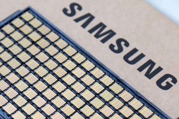
Samsung Electronics is mounting a counterattack in the next-generation high-bandwidth memory (HBM) market by promoting in-house production of base dies. As applying foundry processes to base dies becomes unavoidable starting with HBM4, Samsung’s integrated, turnkey strategy combining design, foundry and packaging is emerging as a point of differentiation from rivals. The industry sees a chance that the structure, in which Samsung lagged an outsourcing-based collaboration model through HBM3E, could be shaken by the shift to HBM4.
Samsung Electronics signed a memorandum of understanding with AMD in March to supply HBM4 as a primary supply for the next-generation AI accelerator Instinct MI455X graphics processing unit (GPU). The two companies also agreed to jointly develop DDR5 for the sixth-generation EPYC CPU, codenamed Venice, and to pursue an exploration of foundry cooperation. The signing ceremony was held at Samsung’s Pyeongtaek campus, where AMD CEO Lisa Su (리사 수) visited South Korea and met Jun Young-hyun (전영현), head of Samsung Electronics’ DS division. Samsung Electronics said it has unmatched, integrated supply capabilities in HBM4 and advanced foundry and packaging.
The possibility that Samsung will supply HBM4 for Nvidia’s next-generation AI accelerator, Vera Rubin, is also growing. Jun met Nvidia CEO Jensen Huang (젠슨 황) on June 8 and discussed ways to broaden cooperation to HBM4E, HBM5 and foundry services.
Samsung, which ceded market share to SK Hynix’s outsourcing-based collaboration model in the HBM3E phase, appears to be trying to change the flow with HBM4. Samsung Electronics is speeding up its catch-up by shipping the world’s first seventh-generation HBM4E samples to Nvidia. Jun, a vice chairman, said, "We will work hard and show you later through results," signaling confidence in the HBM competition.
That confidence is based on a shift in base die processes. From HBM4, applying foundry processes, rather than the existing DRAM process, to base dies has become unavoidable. While global competitors still use a DRAM process for base dies or rely on outsourcing to TSMC, Samsung Electronics has completed in-house base die production by applying its foundry unit’s 4-nanometer FinFET process. According to TechInsights, the share of base die costs in HBM4 is estimated at around 15%. Samsung’s HBM4 has increased bandwidth per cube to 3.3TB/s from the previous generation, and raised data transfer speed to about 13.0Gb/s per pin.
The value of this in-house strategy grows as generations advance. Mirae Asset Securities said the importance of procuring base dies is expected to grow further as products advance to HBM4E and HBM5. It said Samsung’s differentiated strength lies in full-stack manufacturing internalization, handling everything from design to foundry and packaging with its own capabilities. Its business structure, holding both memory and foundry operations, has emerged as a new axis of HBM competition.
HBM4 yields are a variable... warpage challenge remains
This turnkey competitiveness is also seen outside memory. According to the industry, Samsung’s foundry division has been developing Neuralink’s fourth-generation chip for brain implant use on a 4-nanometer process since late last year, led by Elon Musk. One-stop capabilities, handling semiconductor design, foundry and advanced packaging in one place, are cited as the reason behind the order. With big tech orders concentrating on TSMC amid an AI boom and causing foundry bottlenecks, the urgent need to secure a second supply chain is also acting as an opportunity for Samsung.
Still, the shift to HBM4 is not easy. HBM4 is facing a yield decline issue due to wafer warpage, or irregular bending, in base dies and core dies. As the number of stacks rises for higher bandwidth and capacity, individual DRAM dies must be made thinner. With an increase in input-output (I/O) count, connection pitch becomes denser and stress factors concentrate. Hanwha Investment & Securities said it has found that HBM4 yields at the three memory makers are significantly lower than in the previous HBM3E, and this is not a problem limited to a specific company.
Diversification of adoption volume is also a variable. AMD’s MI400, which initially planned to adopt 12-high HBM4 stacks, is now in 8-high and 12-high versions. Nvidia’s Rubin Ultra, which was expected to adopt 16-high HBM4E stacks, is found to be supplied mainly with 12-high stacks. As the number of stacks adopted can vary depending on whether supply capacity is secured, a shortage of memory supply is also likely to affect system specifications.
Ultimately, for the structural advantage of in-house base die production to translate into actual mass-production results, Samsung must first solve yield challenges including warpage. An industry official said, "For Samsung’s turnkey strategy to succeed, it depends on the pace of stabilising HBM4 mass production."