
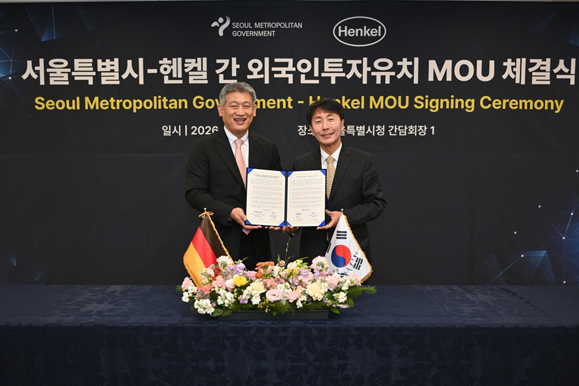
Demand for AI semiconductors and high-bandwidth memory is rising, and a packaging materials research hub will be set up in Seoul. Henkel Korea said on Nov. 10 it signed a business agreement with the Seoul city government on Nov. 9 at Seoul City Hall to establish a semiconductor packaging materials R&D center.
The agreement follows up on a domestic investment plan announced at the 'Invest Korea Summit 2026' held on Nov. 4. Henkel Korea disclosed plans at the time to invest in R&D for advanced packaging materials for AI semiconductors and HBM. It plans to expand its Seoul research center to strengthen capabilities for next-generation packaging materials research and broaden cooperation with South Korea's semiconductor industry.
The company will expand 'Henkel Technology Center Korea' in the Gasan Digital Complex in Seoul's Geumcheon district. The center will be set up in E-Land's building in Gasan-dong. The company said it will pursue foreign direct investment worth about 12.1 billion won and hire about 15 additional research staff.
Research will focus on high-performance electronic adhesives and thermal management materials used to implement AI semiconductors and next-generation HBM. Target materials include liquid molding underfill, which protects semiconductor chips by encasing them in liquid resin, heat dissipation materials, and lead and stiffener bonding materials.
Henkel Korea will also broaden cooperation with South Korea's semiconductor ecosystem. A Henkel Korea official said, "We plan to link our domestic R&D base with our global technology network to broaden support from technology development for advanced packaging materials to providing customer-tailored solutions."
 Daegeon Seok
d2dg@d-today.co.kr